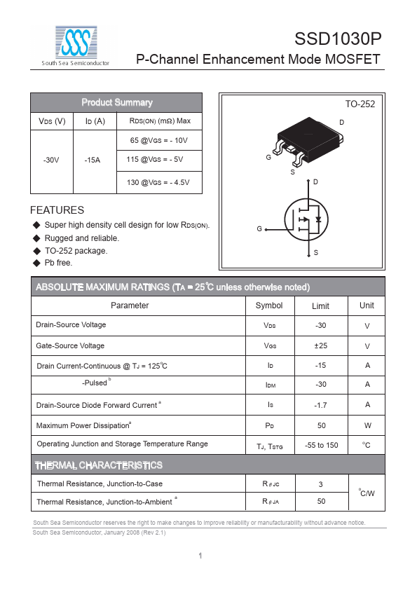
SSD1030P Overview
Key Features
- Super high density cell design for low RDS(ON)
- Rugged and reliable
| Part | SSD1030P |
|---|---|
| Description | P-Channel Enhancement Mode MOSFET |
| Category | MOSFET |
| Manufacturer | South Sea Semiconductor |
| Size | 176.87 KB |
| Part Number | Manufacturer | Description |
|---|---|---|
| SSD1030 | Solomon Systech | Boost Regulating White LED drivers |
| SSD103 | Unknown Manufacturer | Surface-mount Power Transistor |