DESCRIPTION
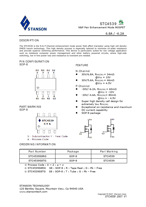
PIN CONFIGURATION SOP-8 PART MARKING SOP-8 FEATURE N-Channel z 30V/6.8A, RDS(ON) = 34mΩ @VGS = 10V z 30V/5.6A, RDS(ON) = 46mΩ @VGS = 4.5V P-Channel z -30V/-6.2A, RDS(ON) = 60mΩ @VGS = -10V z -30V/-4.6A, RDS(ON)= 80mΩ @VGS = - 4.5V z Super high density cell design for extremely low RDS(ON) z Exceptional on-resistance and maximum DC current capability z SOP-8 package ORDERING INFORMATION Part Number Package Part Marking STC4539S8RG SOP-8 STC4539 STC4539S8TG SOP-8 STC4539 ※ Process Code : A ~ Z ; a ~ z ※ STC4539S8RG S8 : SOP-8 ; R : Tape Reel ; G : Pb – Free ※ STC4539S8TG S8 : SOP-8 ; T : Tube ; G : Pb – Free STANSON TECHNOLOGY 120 Bentley Square, Mountain View, Ca 94040 USA Copyright © 2007, Stanson Corp. STC4539 2007. V1 STC4539 N&P Pair Enhancement Mode MOSFET 6.8A / -6.2A ABSOULTE MAXIMUM RATINGS
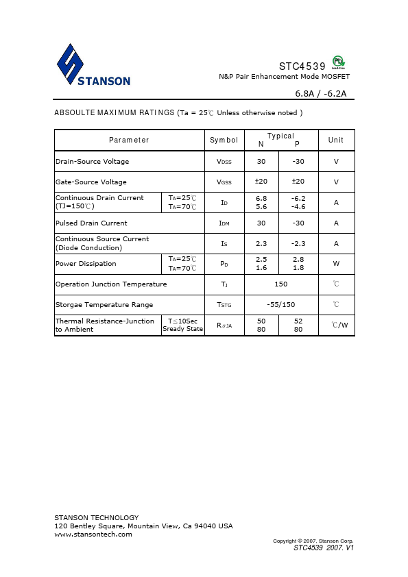
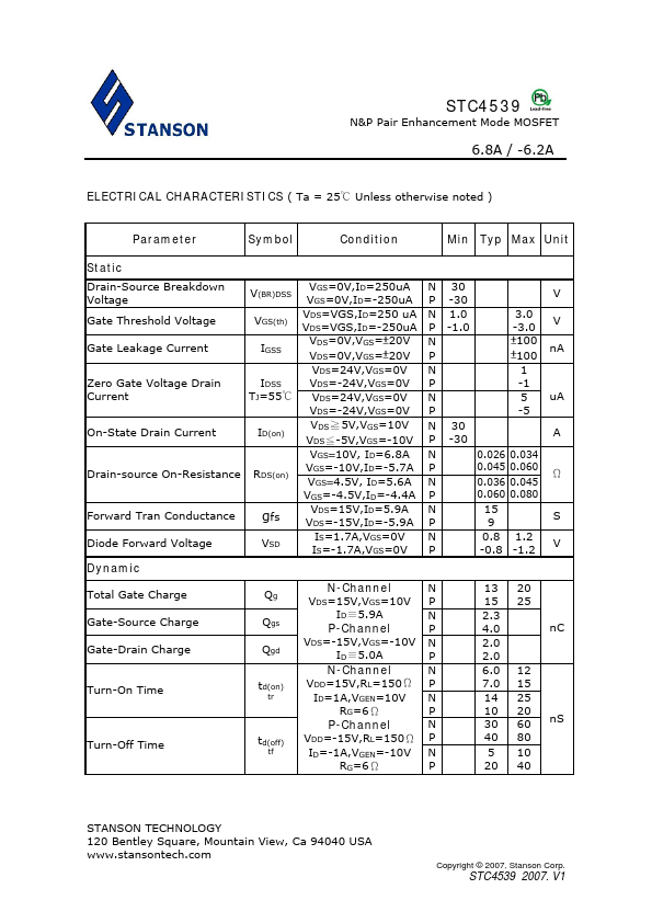
(Ta = 25℃ Unless otherwise noted ) Parameter Symbol Drain-Source Voltage VDSS Gate-Source Voltage Continuous Drain Current (TJ=150℃) TA=25℃ TA=70℃ Pulsed Drain Current Continuous... Stanson Technology