FEATURES
►►±400V input to output isolation ►►±700V isolation between outputs ►►No external voltage supply required ►►Dual isolated output drivers ►►Option of internal or external clock APPLICATIONS
►► Telecommunications ►►Modems ►►Solid state relays ►►High side switches ►►High end audio switches ►► Avionics ►► ATE GENERAL DESCRIPTION
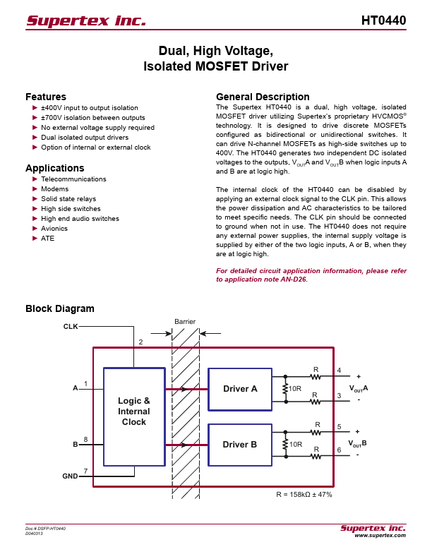
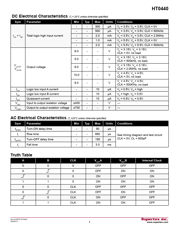
The Supertex The HT0440 generates two independent DC isolated voltages to the outputs, VOUTA and VOUTB when logic inputs A and B are at logic high. The internal clock of the HT0440 can be disabled by applying an external clock signal to the CLK pin. This allows the power dissipation and AC characteristics to be tailored to meet specific needs. The CLK pin should be connected to ground when not in use. The HT0440 does not require any external power supplies, the internal supply voltage is supplied by either of the two logic inputs, A or B, when they are at logic high. For detailed circuit application information, please refer to application note AN-D26. Block Diagram CLK Isolation Barrier 2 A1 B8 GND 7 Logic & Internal Clock Driver A Driver B R 10R R 4 + VOUTA 3- R 10R R 5+ 6 VOUTB - R = 158kΩ ± 47% Doc. Supertex Inc