FEATURES
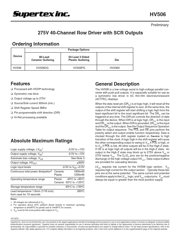
❏ Processed with HVDI technology GENERAL DESCRIPTION
At the same time, the output of the shift register will start shifting a logic high from the least significant bit to the most significant bit. The DRIO can be triggered at any time. The DIR pin controls the direction of data through the device. When DIR is at logic high, DRIOA is the input and DRIOB is the output. When DIR is grounded, DRIOB is the input and the DRIOA is the output. See the Output Sequence Operation Table for output sequence. The POL and OE pins perform the polarity select and output enable function respectively. Data is clocked through the shift register loaded on the low to high transition of the clock. A logic high in the shift register will cause the other corresponding output to swing to VDD if POL is high, or to VSS if POL is low. All other outputs will be in the High-Z state. If OE is at logic high all outputs will be in the High-Z state. An output in the High-Z state may block up to 275V above VSS or 275V below VDD. Supertex Inc