FEATURES
►►High output voltage 80V ►►High speed 5MHz @5.0VDD ►►Low power IBB ≤ 0.1mA (all high) ►►Active pull down 100µA min @25OC ►►Output source current 25mA @60V VBB ►►Each device drives 10 lines ►►High-speed serially-shifted data input ►►5.0V CMOS-compatible inputs ►►Latches on all driver outputs ►►Pin-compatible replacement for UCN5810A and TL4810A, TL4810B APPLICATIONS
►► High speed dot matrix print head driver ►► VFD (vacuum fluorescent display) driver GENERAL DESCRIPTION
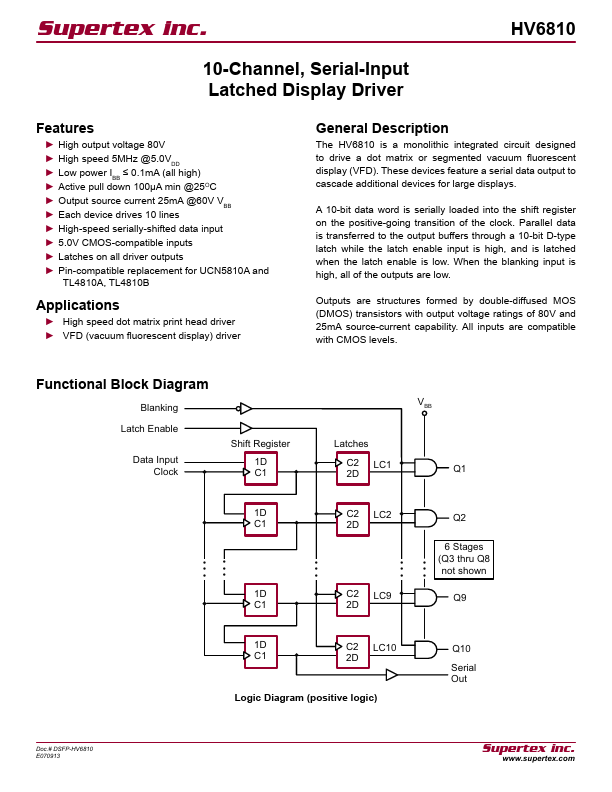
A 10-bit data word is serially loaded into the shift register on the positive-going transition of the clock. Parallel data is transferred to the output buffers through a 10-bit D-type latch while the latch enable input is high, and is latched when the latch enable is low. Outputs are structures formed by double-diffused MOS (DMOS) transistors with output voltage ratings of 80V and 25mA source-current capability. All inputs are compatible with CMOS levels. Functional Block Diagram Blanking Latch Enable Data Inpu... Supertex Inc