FEATURES
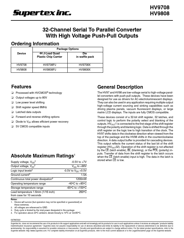
❏ Processed with HVCMOS® technology ❏ Output voltages up to 80V ❏ Low power level shifting ❏ Shift register speed 8MHz ❏ Latched data outputs ❏ Forward and reverse shifting options ❏ Diode to VPP allows efficient power recovery ❏ 5V CMOS compatible inputs GENERAL DESCRIPTION
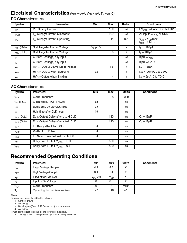
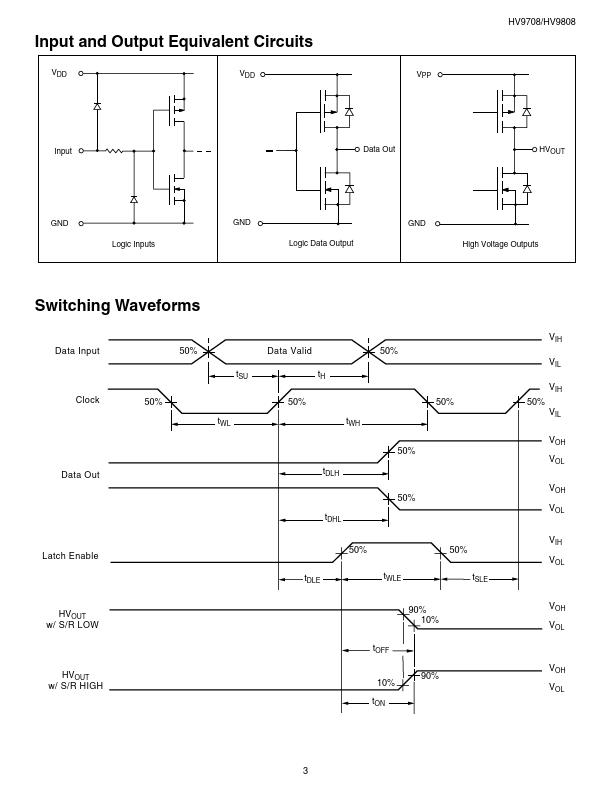
The inputs are fully CMOS compatible. These devices consist of a 32-bit shift register, 32 latches, and control logic to perform the polarity select and blanking of the outputs. HVOUT1 is connected to the first stage of the shift register through the polarity and blanking logic. Data is shifted through the shift register on the logic low to high transition of the clock. The HV97 shifts data in the clockwise direction when viewed from the top of the package and the HV98 shifts in the counterclockwise direction. A data output buffer is provided for cascading devices. This output reflects the current status of the last bit of the shift register (HVOUT32). Operation of the shift register is not affected by the LE (latch enable), BL (blanking), or the POL (polarity) inputs. Supertex Inc