FEATURES
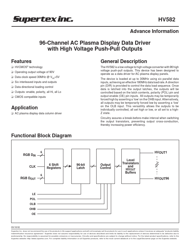
❑ HVCMOS© technology ❑ Operating output voltage of 90V ❑ Data clock speed 30MHz @ VDD=5V ❑ Six interleaved inputs and outputs ❑ Data directional loading control ❑ Outputs: enable, polarity, all Hi, all Lo ❑ CMOS compatible inputs Application ❑ AC plasma display data column driver Functional Block Diagram GENERAL DESCRIPTION
A direction pin (DIR) is provided to control the data load sequence. Once data is latched into the output latches, the outputs will be controlled based on the latch contents, polarity (POL) pin and output enable (OE) pin inputs. All outputs may be temporarily forced high by asserting a ‘low’ on the OHB input. Alternatively, all outputs may be temporarily forced low by asserting a ‘low’ on the OLB input. This versatility allows the outputs to be individually controlled, all set high or low, or all set to a highZ state. Circuitry assures a break-before-make interval when switching the output transistors, preventing output cross-conduction, thereby increasing power efficiency. Supertex