System Logic Semiconductor 74LS06
Hex Inverted Buffers
| Part No. | 74LS06 |
|---|---|
| Datasheet | 74LS06 Download |
| Manufacturer |  System Logic Semiconductor |
| Description | Hex Inverted Buffers |
| Buy | Stock & Price |

MAXIMUM RATINGS
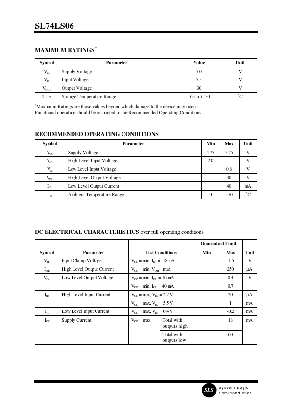
* Symbol VCC VIN VOUT Tstg * Parameter Supply Voltage Input Voltage Output Voltage Storage Temperature Range Value 7.0 5.5 30 -65 to +150 Unit V V V °CMAXIMUM RATINGS
are those values beyond which damage to the device may occur. Functional operation should be restricted to the Recommended Operating Conditions. RECOMMENDED OPERATING CONDITIONS Symbol VCC VIH VIL VOH IOL TA Supply Voltage High Level Input Voltage Low Level Input Voltage High Level Output Voltage Low Level Output Current Ambient Temperature Range 0 Parameter Min 4.75 2.0 0.8 30 40 +70 Max 5.25 Unit V V V V mA °C DCELECTRICAL CHARACTERISTICS
over full operating conditions Guaranteed Limit Symbol VIK IOH VOL Parameter Input Clamp Voltage High Level Output Current Low Level Output Voltage Test Conditions VCC = min, IIN = -18 mA VCC = min, VOH= max VCC = min, IOL = 16 mA VCC = min, IOL = 40 mA IIH High Level Input Current VCC = max, VIN = 2.7 V VCC = max, VIN = 5.5 V IIL ICC Low Level Input Current Supply Cu...