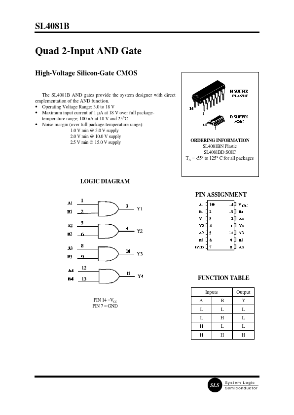
SL4081B
SL4081B is Quad 2-Input AND Gate manufactured by System Logic Semiconductor.
Quad 2-Input AND Gate
High-Voltage Silicon-Gate CMOS
The SL4081B AND gates provide the system designer with direct emplementation of the AND function.
- Operating Voltage Range: 3.0 to 18 V
- Maximum input current of 1 µA at 18 V over full packagetemperature range; 100 n A at 18 V and 25°C
- Noise margin (over full package temperature range): 1.0 V min @ 5.0 V supply 2.0 V min @ 10.0 V supply 2.5 V min @ 15.0 V supply
ORDERING INFORMATION SL4081BN Plastic SL4081BD SOIC TA = -55° to 125° C for all packages
LOGIC DIAGRAM PIN ASSIGNMENT
FUNCTION TABLE
Inputs PIN 14 =VCC PIN 7 = GND A L L H H B L H L H Output Y L L L H
System Logic Semiconductor
MAXIMUM RATINGS
- Symbol VCC VIN VOUT IIN PD PD Tstg TL
- Parameter DC Supply Voltage (Referenced to GND) DC Input Voltage (Referenced to GND) DC Output Voltage (Referenced to GND) DC Input Current, per Pin Power Dissipation in Still Air, Plastic DIP+ SOIC Package+ Power Dissipation per Output Transistor Storage Temperature Lead Temperature, 1 mm from Case for 10 Seconds (Plastic DIP or SOIC Package)
Value -0.5 to +20 -0.5 to VCC +0.5 -0.5 to VCC +0.5 ±10 750 500 100 -65 to +150 260
Unit V V V m A m W m W °C °C
Maximum Ratings are those values beyond which damage to the device may occur. Functional operation should be restricted to the Remended Operating Conditions. +Derating
- Plastic DIP:
- 10 m W/°C from 65° to 125°C SOIC Package: :
- 7 m W/°C from 65° to 125°C
REMENDED OPERATING CONDITIONS
Symbol VCC VIN, VOUT TA Parameter DC Supply Voltage (Referenced to GND) DC Input Voltage, Output Voltage (Referenced to GND) Operating Temperature, All Package Types Min 3.0 0 -55 Max 18 VCC +125 Unit V V °C
This device contains protection circuitry to guard against damage due to high static voltages or electric fields. However, precautions must be taken to avoid applications of any voltage higher than maximum rated voltages to this high-impedance circuit. For proper operation, VIN and VOUT should be...