SL74LS164
SL74LS164 is 8-Bit Serial-Input/Parallel-Output Shift Register manufactured by System Logic Semiconductor.
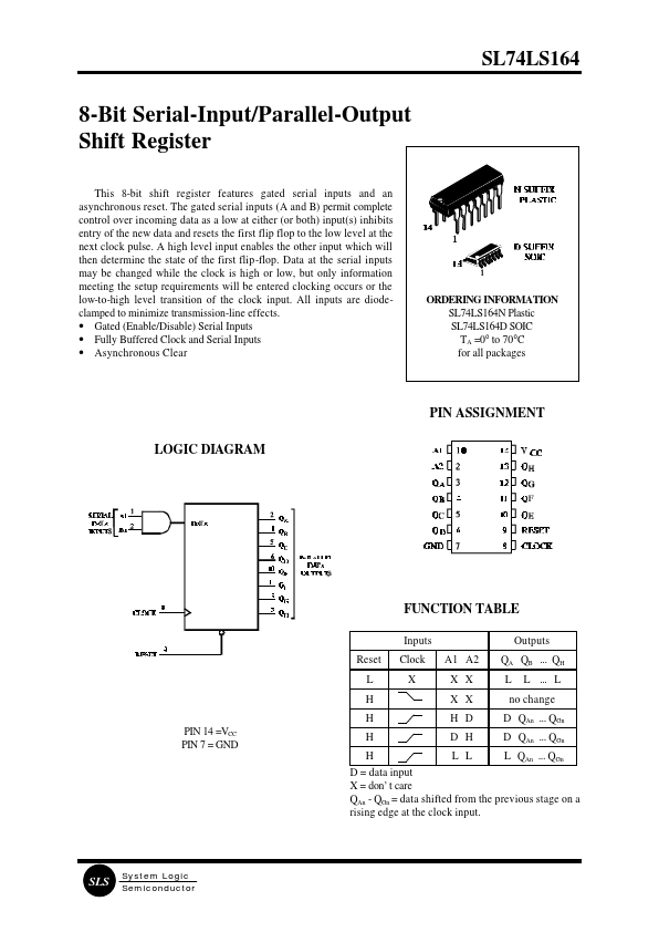
features gated serial inputs and an asynchronous reset. The gated serial inputs (A and B) permit plete control over ining data as a low at either (or both) input(s) inhibits entry of the new data and resets the first flip flop to the low level at the next clock pulse. A high level input enables the other input which will then determine the state of the first flip-flop. Data at the serial inputs may be changed while the clock is high or low, but only information meeting the setup requirements will be entered clocking occurs or the low-to-high level transition of the clock input. All inputs are diodeclamped to minimize transmission-line effects.
- Gated (Enable/Disable) Serial Inputs
- Fully Buffered Clock and Serial Inputs
- Asynchronous Clear
ORDERING INFORMATION SL74LS164N Plastic SL74LS164D SOIC TA =0° to 70°C for all packages
PIN ASSIGNMENT LOGIC DIAGRAM
FUNCTION TABLE
Inputs Reset L H H PIN 14 =VCC PIN 7 = GND H H Clock X A1 A2 X X X X H D D H L L Outputs QA QB ... QH L L ... L no change D QAn ... QGn D QAn ... QGn L QAn ... QGn
D = data input X = don’t care QAn
- QGn = data shifted from the previous stage on a rising edge at the clock input.
System Logic Semiconductor
MAXIMUM RATINGS
- Symbol VCC VIN VOUT Tstg
- Parameter Supply Voltage Input Voltage Output Voltage Storage Temperature Range
Value 7.0 7.0 5.5 -65 to +150
Unit V V V °C
Maximum Ratings are those values beyond which damage to the device may occur. Functional operation should be restricted to the Remended Operating Conditions.
REMENDED OPERATING CONDITIONS
Symbol VCC VIH VIL IOH IOL TA fclock tsu th tw tw trec Supply Voltage High Level Input Voltage Low Level Input Voltage High Level Output Current Low Level Output Current Ambient Temperature Range Clock Frequency Setup Time, A1 or A2 to Clock Hold Time, Clock to A1 or A2 Pulse Width, Clock Pulse Width, Reset Recovery Time 0 0 15 5 20 20 5 Parameter Min 4.75 2.0 0.8 -0.4 8.0 +70 25 Max 5.25 Unit V V V m A m A °C MHz ns ns...