SL74LS245
SL74LS245 is Octal 3-State Noninverting Bus Transceiver manufactured by System Logic Semiconductor.
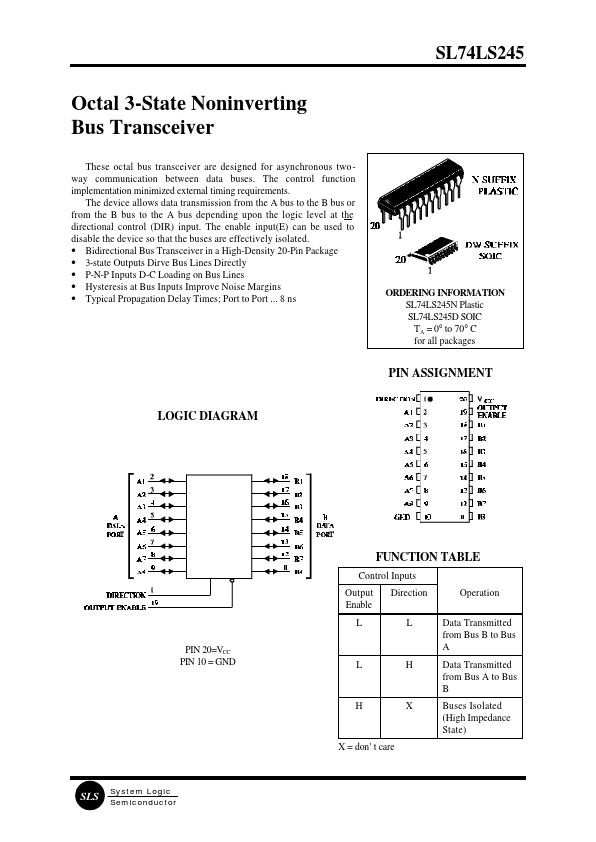
Octal 3-State Noninverting Bus Transceiver
These octal bus transceiver are designed for asynchronous twoway munication between data buses. The control function implementation minimized external timing requirements. The device allows data transmission from the A bus to the B bus or from the B bus to the A bus depending upon the logic level at the directional control (DIR) input. The enable input(E) can be used to disable the device so that the buses are effectively isolated.
- Bidirectional Bus Transceiver in a High-Density 20-Pin Package
- 3-state Outputs Dirve Bus Lines Directly
- P-N-P Inputs D-C Loading on Bus Lines
- Hysteresis at Bus Inputs Improve Noise Margins
- Typical Propagation Delay Times; Port to Port ... 8 ns
ORDERING INFORMATION SL74LS245N Plastic SL74LS245D SOIC TA = 0° to 70° C for all packages
PIN ASSIGNMENT
LOGIC DIAGRAM
FUNCTION TABLE
Control Inputs Output Enable L PIN 20=VCC PIN 10 = GND Direction L Operation Data Transmitted from Bus B to Bus A Data Transmitted from Bus A to Bus B Buses Isolated (High Impedance State)
X = don’t care
System Logic Semiconductor
MAXIMUM RATINGS
- Symbol VCC VIN VOUT Tstg
- Parameter Supply Voltage Input Voltage Output Voltage Storage Temperature Range
Value 7.0 7.0 5.5 -65 to +150
Unit V V V °C
Maximum Ratings are those values beyond which damage to the device may occur. Functional operation should be restricted to the Remended Operating Conditions.
REMENDED OPERATING CONDITIONS
Symbol VCC VIH VIL IOH IOL TA Supply Voltage High Level Input Voltage Low Level Input Voltage High Level Output Current Low Level Output Current Ambient Temperature Range 0 Parameter Min 4.75 2.0 0.8 -15 24 +70 Max 5.25 Unit V V V m A m A °C
DC ELECTRICAL CHARACTERISTICS over full operating conditions
Guaranteed Limit Symbol VIK VOH Parameter Input Clamp Voltage High Level Output Voltage Test Conditions VCC = min, IIN = -18 m A VCC = min, IOH = -1.0 m A VCC = min, IOH = -3.0 m A VCC = min, IOH...