DESCRIPTION
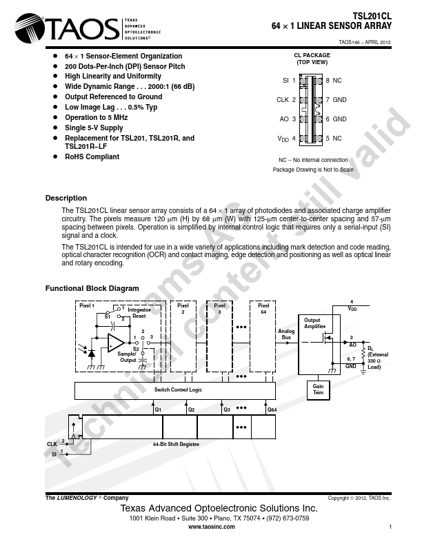
Operation is simplified by internal control logic that requires only a serial-input (SI) signal and a clock. Functional Block Diagram Pixel 1 S1 1 Integrator 2 Reset 2 _ 13 + S2 Sample/ Output Pixel 2 Pixel 3 Switch Control Logic Q1 Q2 Q3 Pixel 64 Analog Bus Output Amplifier Gain Trim Q64 4 VDD 3 AO 6, 7 GND RL (External 330 W Load) 2 CLK SI 1 64-Bit Shift Register The LUMENOLOGY r Company r Texas Advanced Optoelectronic Solutions Inc. 1001 Klein Road S Suite 300 S Plano, TX 75074 S (972r) 673-0759 Copyright E 2012, TAOS Inc. 1 Technical coantmesntAsGtill valid TSL201CL 64 y 1 LINEAR SENSOR ARRAY TAOS146 − APRIL 2012 Terminal Functions TERMINAL NAME NO. AO 3 CLK 2 GND 6, 7 SI 1 VDD 4 DESCRIPTION
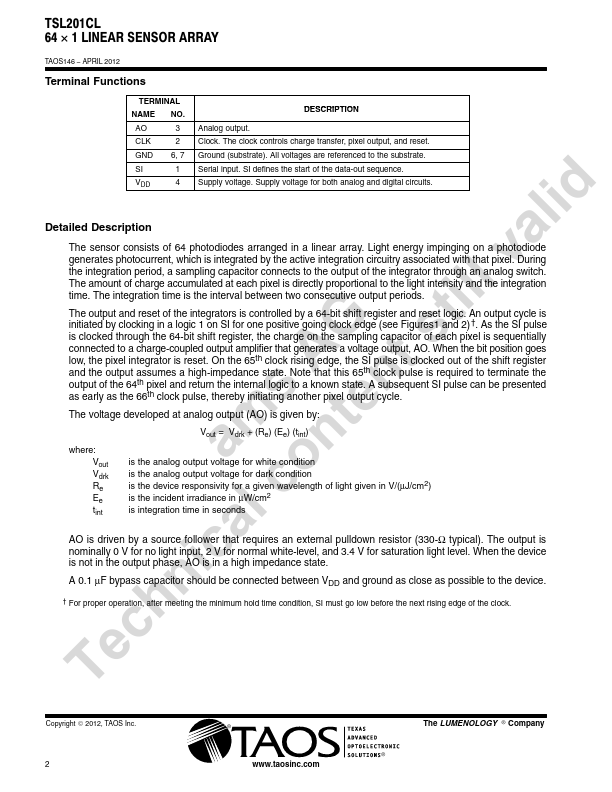
Analog output. Clock. The clock controls charge transfer, pixel output, and reset. Ground (substrate). All voltages are referenced to the substrate. Serial input. SI defines the start of the data-out sequence. Supply voltage. Supply voltage for both analog and digital circuits. Detailed DESCRIPTION
The sensor consists of 64 photodiodes arranged in a linear array. TAOS