Datasheet Summary
TECH MOS Technology. Dual P-Channel High Density Trench MOSFET
TM4953S TM4953FS(Pb-free)
PRODUCT SUMMARY
VDSS
ID RDS(on) (m-ohm) Max
- 30V
- 4.9A
- 3.6A
53 @ VGS =
- 10V 95 @ VGS =
- 4.5V
Features
- Super high dense cell trench design for low RDS(on).
- Rugged and reliable.
- Surface Mount package.
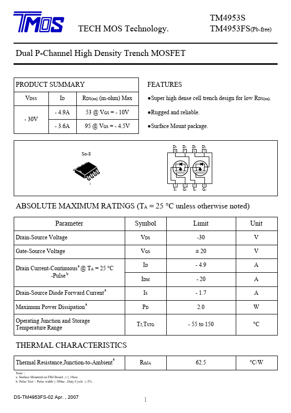
So-8
D1 D1 D2 D2
876 5
1 1234
S1 G1 S2...