FEATURES
D D D D "15 V Input Signal Range 44-V Maximum Supply Ranges On-Resistance: 45 W TTL and CMOS Compatibility Benefits D Wide Dynamic Range D Simple Interfacing D Reduced External Component Count APPLICATIONS
D D D D Servo Control Switching Programmable Gain Amplifiers Audio Switching Programmable Filters DESCRIPTION
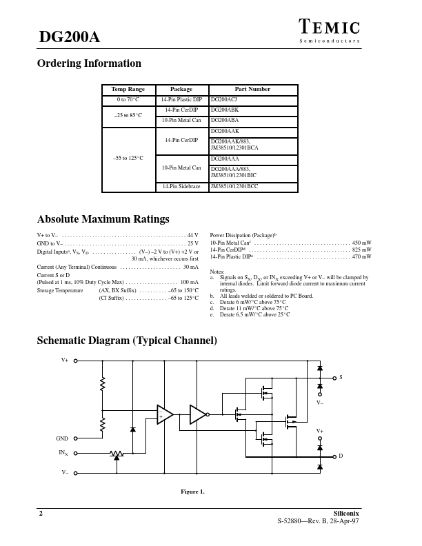
An epitaxial layer prevents latchup. Each switch conducts equally well in both directions when on, and blocks up to 30 V peak-to-peak when off. In the on condition, this bi-directional switch introduces no offset voltage of its own. Functional Block Diagram and Pin Configuration Dual-In-Line IN2 NC GND NC S2 D2 V– 1 2 3 4 5 6 7 Top View 14 13 12 11 10 9 8 IN1 NC V+ Substrate NC S1 D1 NC GND IN2 2 3 4 S2 5 6 V– IN1 1 Metal Can V+ (Substrate and Case) 10 S1 9 8 7 D1 NC D2 Top View Truth Table Logic 0 1 Logic g “0” v 0.8 V L i “1” w 2.4 Logic 24V Switch ON OFF Updates to this data sheet may be obtained via facsimile by calling Siliconix FaxBack, 1-408-970-5600. Please request FaxBack document #70035. TEMIC Semiconductors