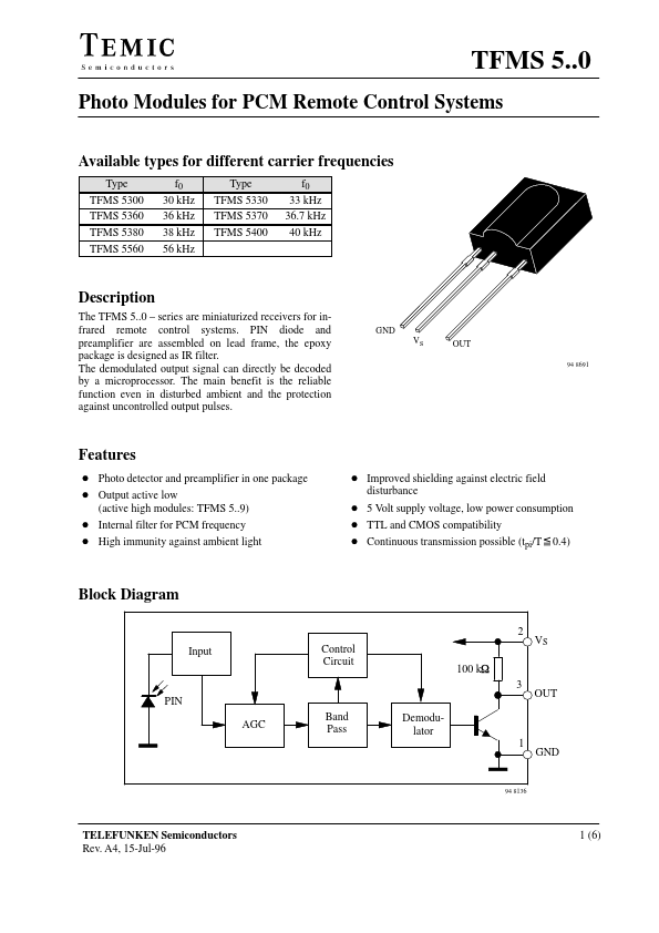
DESCRIPTION
PIN diode and preamplifier are assembled on lead frame, the epoxy package is designed as IR filter. GND VS OUT 94 8691 FEATURES
D Photo detector and preamplifier in one package D Output active low (active high modules: TFMS 5..9) D Improved shielding against electric field disturbance D Internal filter for PCM frequency D High immunity against ambient light D 5 Volt supply voltage, low power consumption D TTL and CMOS compatibility D Continuous transmission possible (tpi/T 0.4) x Block Diagram 2 Input Control Circuit 100 kW 3 PIN AGC Band Pass Demodulator 1 GND OUT VS 94 8136 TELEFUNKEN Semiconductors Rev. A4, 15-Jul-96 1 (6) TFMS 5..0 ABSOLUTE MAXIMUM RATINGS
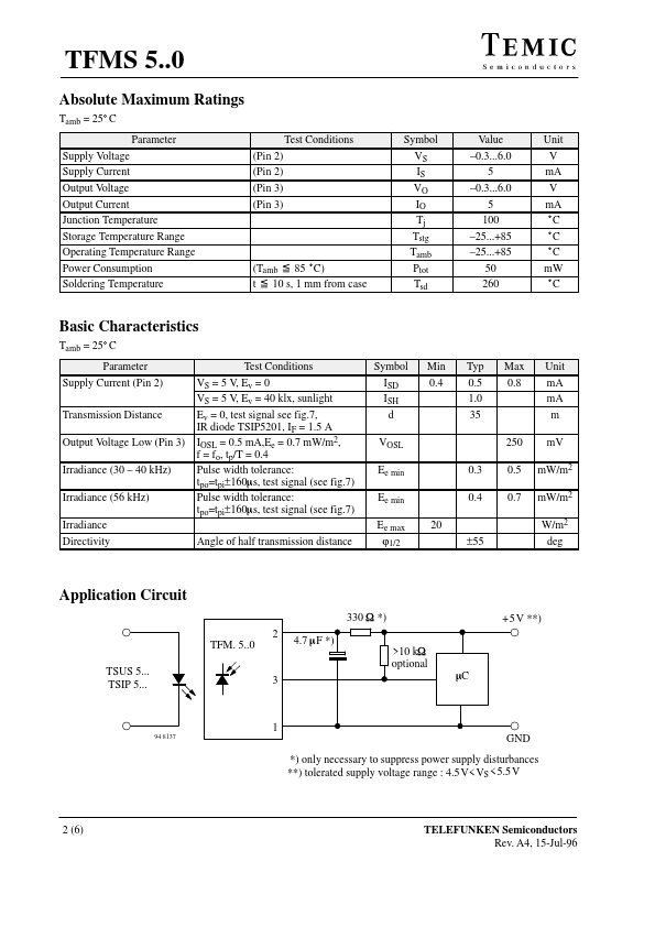
Tamb = 25_C Parameter Supply Voltage Supply Current Output Voltage Output Current Junction Temperature Storage Temperature Range Operating Temperature Range Power Consumption Soldering Temperature (Pin 2) (Pin 2) (Pin 3) (Pin 3) Test Conditions Symbol VS IS VO IO Tj Tstg Tamb Ptot Tsd Value –0.3...6.0 5 –0.3...6.0 5 1... TEMIC Semiconductors