DESCRIPTION
A double balanced approach was chosen to assure good isolation characteristics and a minimum of spurious products. No output transformer or balun is required. FEATURES
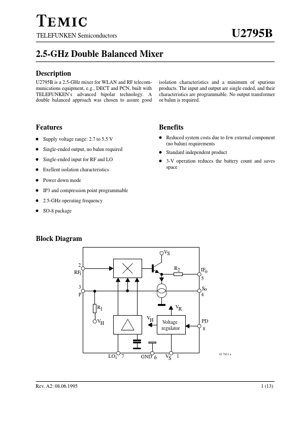
D Supply voltage range: 2.7 to 5.5 V D Single-ended output, no balun required D Single-ended input for RF and LO D Exellent isolation characteristics D Power down mode D IP3 and compression point programmable D 2.5-GHz operating frequency D SO-8 package Benefits D Reduced system costs due to few external component (no balun) requirements D Standard independent product D 3-V operation reduces the battery count and saves space Block Diagram VS 2 RFi 3 P R1 VH VH VR Voltage regulator PD 8 R2 IFo 5 So 4 LO i 7 GND 6 VS 1 93 7811 e Rev. A2: 08.06.1995 1 (13) U2795B Pin DESCRIPTION
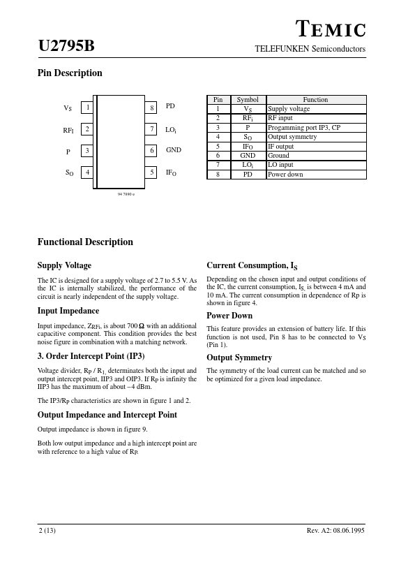
Pin 1 2 3 4 5 6 7 8 TELEFUNKEN Semiconductors VS RFI P SO 1 2 3 4 94 7890 e 8 7 6 5 PD LOi GND IFO Symbol VS RFi P SO IFO GND LOi PD Function Supply voltage RF input Progamming port IP3, CP Output symmetry IF output Ground LO input Power down Functional DESCRIPTION
Supply Voltage The IC is designed for a supply voltage of 2.7 to 5.5 V. TEMIC Semiconductors