DESCRIPTION
FEATURES
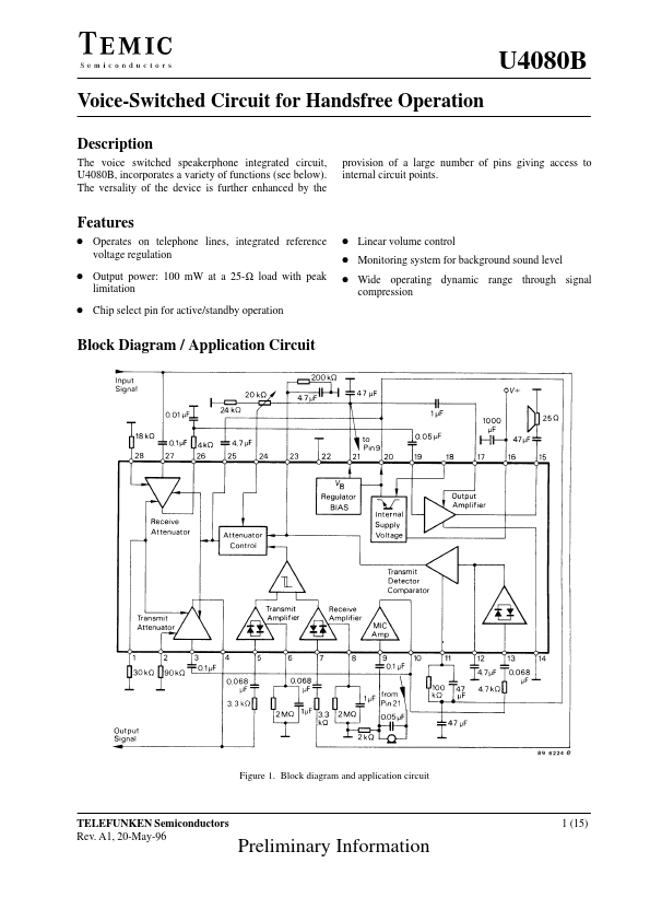
D Operates on telephone lines, integrated reference voltage regulation D Output power: 100 mW at a 25-Ω load with peak limitation D Linear volume control D Monitoring system for background sound level D Wide operating dynamic range through signal compression D Chip select pin for active/standby operation Block Diagram / Application Circuit Figure 1. Block diagram and application circuit TELEFUNKEN Semiconductors Rev. A1, 20-May-96 1 (15) Preliminary Information U4080B Pin DESCRIPTION
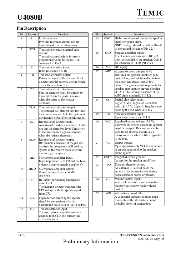
Pin 1 Symbol Function R1 Load resistance. Pin 14 Symbol Function GND1 High current ground pin for the speaker 2 RTG 3 4 TI TO 5 TLI 6 TLO 7 RLI 8 RLO 9 MIC 10 MICO 11 CP1 12 CP2 13 TDI Provides reference current for the transmit and receive attenuators. Transmit attenuator nominal gain resistor. Transmit channel gain is inversely proportional to the resistance RTG connected to Pin 2. Transmit attenuator input. Input resistance is 5 kΩ Transmit attenuator output. Drives the input of the transmit level detector and the external circuit which drives the telephone line. TEMIC Semiconductors