DESCRIPTION
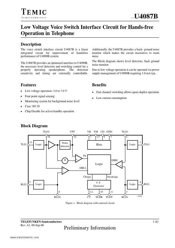
The voice switch interface circuit Additionally, the U4087B provides a back- ground noise monitor which makes the circuit insensitive to room noise. The Block diagram shows level detectors, back ground noise monitor. Due to low voltage operation it can be operated via power supply management of U4090B requiring 1.0 mA typ. FEATURES
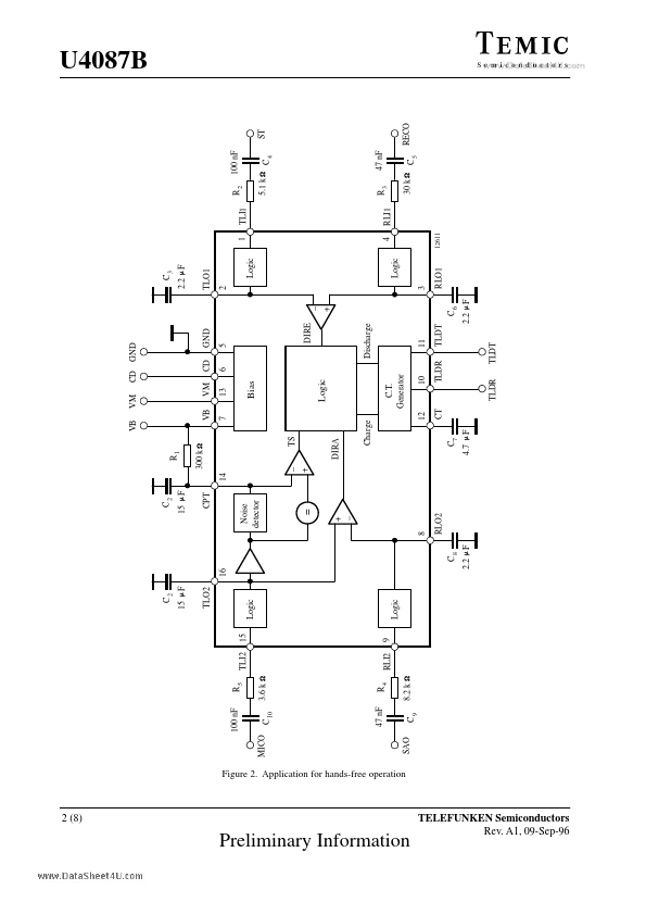
D Low voltage operation: 3.0 to 7.0 V D Four point signal sensing D Monitoring system for background noise level D Case: SO 16 D Chip Disable for active/standby operation Benefits D Fast channel switching allows quasi duplex operation D Low current consumption Block Diagram TLO2 16 TLI2 15 Logic Noise detector CPT 14 VB 7 VM 13 CD GND 6 5 TLO1 2 Logic 1 TLI1 Bias = + – – + TS DIRE Logic DIRA Charge RLI2 9 Logic 8 RLO2 12 CT C.T. Generator 10 TLDR 11 TLDT Discharge – + Logic 3 RLO1 4 RLI1 12610 Figure 1. Block diagram with external circuit TELEFUNKEN Semiconductors Rev. A1, 09-Sep-96 1 (8) Preliminary Information U4087B 2 (8) VB VM CD GND C2 15 TL... TEMIC Semiconductors