DESCRIPTION
After successful triggering and the following delay time, an ignition pulse at the output is released. A further triggering is only possible after the elapse of the delay time. FEATURES
D D D D D L D1 1N4007 R1 Vmains 230 V 24 kW/ 2W R3 220 kW C3 1.5 nF APPLICATIONS
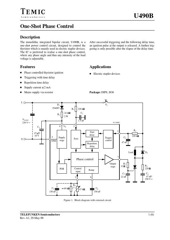
D Electric stapler devices Phase controlled thyristor ignition Triggering with time delay Repetition time delay Supply current x2 mA Package: DIP8, SO8 Mains supply via resistor S1 X C1 47 mF/ 10 V 8 VS 3 4 GND 95 10866 Start delay Supply stage Sync. Repetition delay Trigger control 2 C2 47 nF R2 220 kW N Load D2 Phase control POR Control input 5 R5 W 7 Output stage R7 33 W C7 22 nF Ramp 6 R4 220 W C4 47 nF/ 250 V X C5 150 nF [68 k 47 kW C6 150 nF Figure 1. Block diagram with external circuit TELEFUNKEN Semiconductors Rev. A1, 29-May-96 1 (6) U490B Pin DESCRIPTION
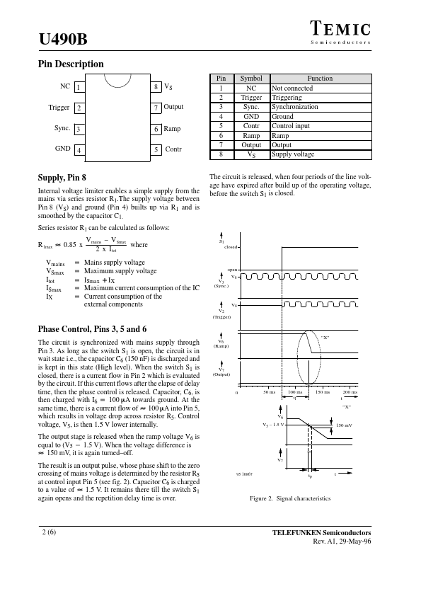
NC 1 Trigger 2 8 VS 7 Output 6 Ramp 5 Contr Pin 1 2 3 4 5 6 7 8 Symbol NC Trigger Sync. GND Contr Ramp Output VS Function Not connected Triggering Synchronization Ground Control input Ramp Output Supply voltage Sync. TEMIC Semiconductors