DESCRIPTION
FEATURES
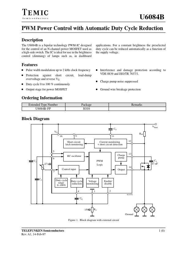
D Pulse width modulation up to 2 kHz clock frequency D Protection against short circuit, load-dump overvoltage and reverse VS D Interference and damage protection according to VDE 0839 and ISO/TR 7637/1. D Duty cycle 0 to 100 % continuously D Output stage for power MOSFET D Charge pump noise suppressed D Ground wire breakage protection Ordering Information Extended Type Number U6084B–FP Package SO16 Remarks Block Diagram C5 VS 16 9 Short circuit latch monitoring 5 6 C1 47 kW 3 C2 Control input RC oscillator PWM Logic Output 14 Charge pump 13 C3 47 nF 11 Current monitoring + short circuit detection 12 Rsh VBatt Duty cycle range 0–100% Duty cycle reduction 4 C6 Voltage monitoring 1 Enable/ disable 2 95 9751 150W R3 Ground Figure 1. Block diagram with external circuit TELEFUNKEN Semiconductors Rev. A1, 14-Feb-97 1 (8) U6084B Pin DESCRIPTION
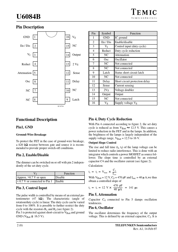
GND En / Dis VI Reduct 1 2 3 4 16 15 14 13 12 11 10 9 95 9754 VS NC Output 2 VS Sense Delay NC Latch Attenuation 5 Osc NC NC 6 7... TEMIC Semiconductors