DESCRIPTION
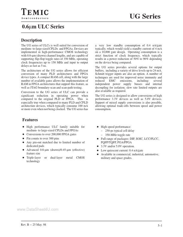
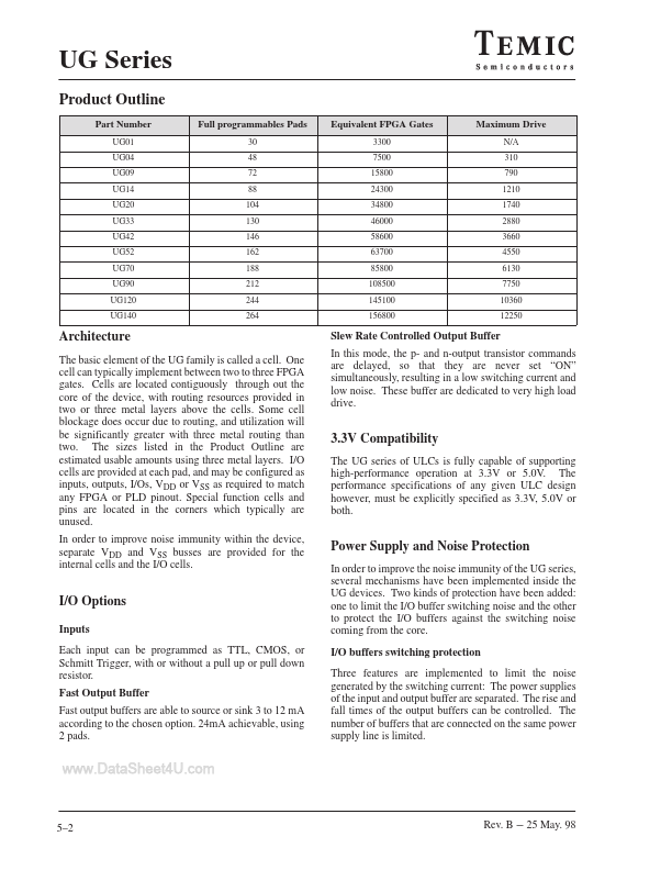
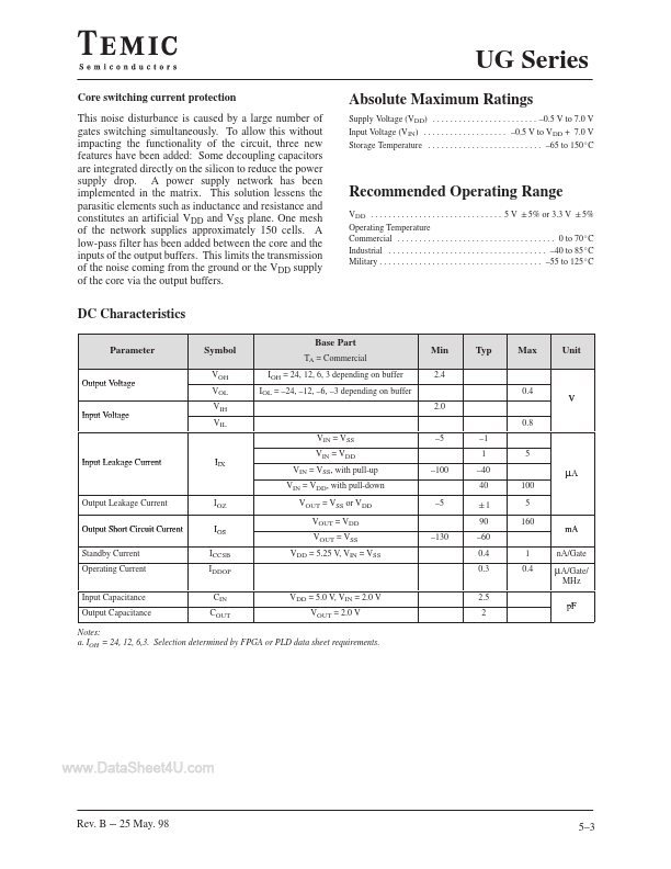
Devices are implemented in high-performance CMOS technology with 0.6-µm (drawn) channel lengths, and are capable of supporting flip-flop toggle rates of 350 MHz, operating clock frequencies up to 150 MHz and input to output delays as fast as 5 ns. A compact RAM cell, along with the large number of available gates allows the implementation of RAM in FPGA architectures that support this feature, as well as JTAG boundary-scan and scan-path testing. Conversion to the UG series of ULC can provide a significant reduction in operating power when compared to the original PLD or FPGA. This is especially true when compared to many PLD and CPLD architecture devices, which typically consume 100 mA or more even when not being clocked. The UG series has a very low standby consumption of 0.4 nA/gate typically, which would yield a standby current of 4 mA on a 10,000 gate design. Operating consumption is a strict function of clock frequency, which typically results in a power reduction of 50% to 90% depending on the device being compared. TEMIC Semiconductors