THC63LVDF84B Description
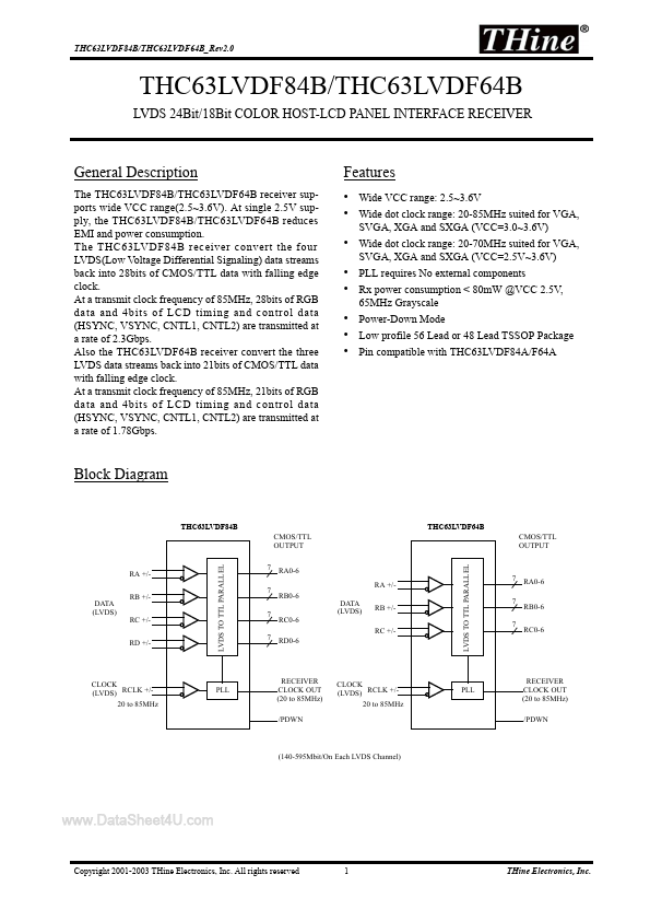
The THC63LVDF84B/THC63LVDF64B receiver supports wide VCC range(2.5~3.6V). At single 2.5V supply, the THC63LVDF84B/THC63LVDF64B reduces EMI and power consumption. The THC63LVDF84B receiver convert the four LVDS(Low Voltage Differential Signaling) data streams back into 28bits of CMOS/TTL data with falling edge clock.
THC63LVDF84B Key Features
- Wide VCC range: 2.5~3.6V
- Wide dot clock range: 20-85MHz suited for VGA
- SVGA, XGA and SXGA (VCC=3.0~3.6V) Wide dot clock range: 20-70MHz suited for VGA, SVGA, XGA and SXGA (VCC=2.5V~3.6V)
- PLL requires No external ponents
- Rx power consumption < 80mW @VCC 2.5V
- Power-Down Mode
- Low profile 56 Lead or 48 Lead TSSOP Package
- Pin patible with THC63LVDF84A/F64A