TW045Z120C
TW045Z120C is Silicon Carbide N-Channel MOSFET manufactured by Toshiba.
Features
(1) Chip design of 3rd generation (Built-in Si C schottky barrier diode) (2) Low diode forward voltage: VDSF = -1.35 V (typ.) (3) High voltage: VDSS = 1200 V (4) Low drain-source on-resistance: RDS(ON) = 45 mΩ (typ.) (5) Less susceptible to malfunction due to high threshold voltage: Vth = 3.0 to 5.0 V (VDS = 10 V, ID = 6.7 m A) (6) Remended gate
- source drive voltage: VGS_on = 18 V, VGS_off = 0 V (7) Enhancement mode.
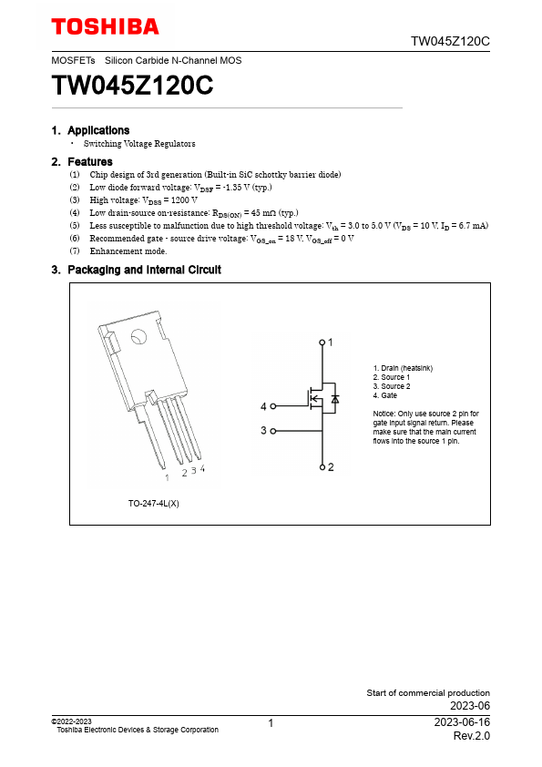
3. Packaging and Internal Circuit
TO-247-4L(X)
1. Drain (heatsink) 2. Source 1 3. Source 2 4. Gate
Notice: Only use source 2 pin for gate input signal return. Please make sure that the main current flows into the source 1 pin.
©2022-2023
Toshiba Electronic Devices & Storage Corporation
Start of mercial production
2023-06
2023-06-16 Rev.2.0
4. Absolute Maximum Ratings (Note) (Ta = 25
- unless otherwise specified)
Characteristics
Symbol
Rating
Unit
Drain-source voltage Gate-source voltage Drain current (DC) Drain current (DC) Drain current (pulsed) Drain current (pulsed) Power dissipation Channel temperature Storage temperature Mounting torque
( Tc = 25
- ) ( Tc = 100- ) ( Tc = 25
- ) ( Tc = 100- ) ( Tc = 25- )
(Note 1) (Note 1) (Note 1) (Note 1)
VDSS VGSS
ID ID IDP IDP PD Tch Tstg TOR
1200 +25/-10
40 30 114 82 182 175 -55 to 175 0.8
- N- m
Note:
Using continuously under heavy loads (e.g. the application of high temperature/current/voltage and the significant change in temperature, etc.) may cause this product to decrease in the reliability significantly even if the operating conditions (i.e. operating temperature/current/voltage, etc.) are within the absolute maximum ratings. Please design the appropriate reliability upon reviewing the Toshiba Semiconductor Reliability Handbook ("Handling Precautions"/"Derating Concept and Methods") and individual reliability data (i.e. reliability test report and estimated failure rate, etc).
5. Thermal Characteristics
Characteristics Channel-to-case thermal resistance...