3DA752
FEATURES
Power dissipation PCM: 1.2 W (Tamb=25℃)
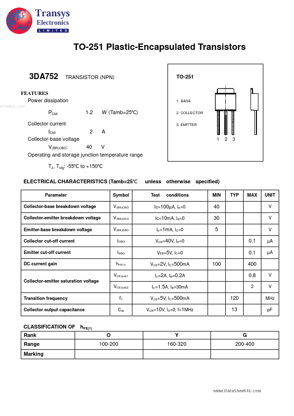
1. BASE 2. COLLECTOR 3. EMITTER a Sheet4U.
Collector current 2 A ICM: Collector-base voltage 40 V V(BR)CBO: Operating and storage junction temperature range TJ, Tstg: -55℃ to +150℃ ELECTRICAL CHARACTERISTICS (Tamb=25℃
Parameter Collector-base breakdown voltage Collector-emitter breakdown voltage Emitter-base breakdown voltage Collector cut-off current Emitter cut-off current DC current gain Symbol V(BR)CBO V(BR)CEO V(BR)EBO ICBO IEBO h FE(1) VCE(sat)1 Collector-emitter saturation voltage VCE(sat)2 Transition frequency Collector output capacitance
3 unless otherwise specified)
Test conditions MIN TYP MAX UNIT V V V
Ic=100µA, IE=0 Ic=10m A, IB=0 IE=1m A, IC=0 VCB=40V, IE=0 VEB=5V, IC=0 VCE=2V, IC=500m A IC=2A, IB=0.2A IC=1.5A, IB=30m A VCE=5V, IC=500m A VCB=10V, IE=0, f=1MHz
40 30 5 0.1 0.1 100 400 0.8
µA µA
V V MHz p F f T
Cob
120 13
CLASSIFICATION OF h FE(1) Rank Range Marking O 100-200 Y 160-320 G...