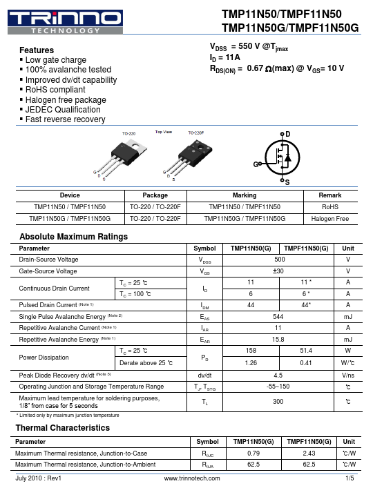
Datasheet4U Logo Datasheet4U.com

TMPF11N50 - N-channel MOSFET

Download the TMPF11N50 datasheet PDF. This datasheet also covers the TMP11N50 variant, as both devices belong to the same n-channel mosfet family and are provided as variant models within a single manufacturer datasheet.

Key Features

  • Low gate charge.
  • 100% avalanche tested.
  • Improved dv/dt capability.
  • RoHS compliant.
  • Halogen free package.
  • JEDEC Qualification.
  • Fast reverse recovery TMP11N50/TMPF11N50 TMP11N50G/TMPF11N50G VDSS = 550 V @Tjmax ID = 11A RDS(ON) = 0.67 W(max) @ VGS= 10 V D G Device TMP11N50 / TMPF11N50 TMP11N50G / TMPF11N50G Package TO-220 / TO-220F TO-220 / TO-220F S Marking TMP11N50 / TMPF11N50 TMP11N50G / TMPF11N50G Remark RoHS Halogen Free Absolute Maximum Ratings Para.

📥 Download Datasheet

Note: The manufacturer provides a single datasheet file (TMP11N50-TRinno.pdf) that lists specifications for multiple related part numbers.

Datasheet Details

Part number TMPF11N50
Manufacturer TRinno
File Size 343.77 KB
Description N-channel MOSFET
Datasheet download datasheet TMPF11N50 Datasheet

Full PDF Text Transcription for TMPF11N50 (Reference)

Note: Below is a high-fidelity text extraction (approx. 800 characters) for TMPF11N50. For precise diagrams, tables, and layout, please refer to the original PDF.

Features  Low gate charge  100% avalanche tested  Improved dv/dt capability  RoHS compliant  Halogen free package  JEDEC Qualification  Fast reverse recovery TMP11...

View more extracted text
logen free package  JEDEC Qualification  Fast reverse recovery TMP11N50/TMPF11N50 TMP11N50G/TMPF11N50G VDSS = 550 V @Tjmax ID = 11A RDS(ON) = 0.