TMPF3N50AZ
Features
- Low gate charge
- 100% avalanche tested
- Improved dv/dt capability
- Ro HS pliant
- Halogen free package
- JEDEC Qualification
- Improved ESD performance
TMP3N50AZ(G)/TMPF3N50AZ(G)
BVDSS 500V
N-channel MOSFET
ID RDS(on)
2.5A
< 2.8W
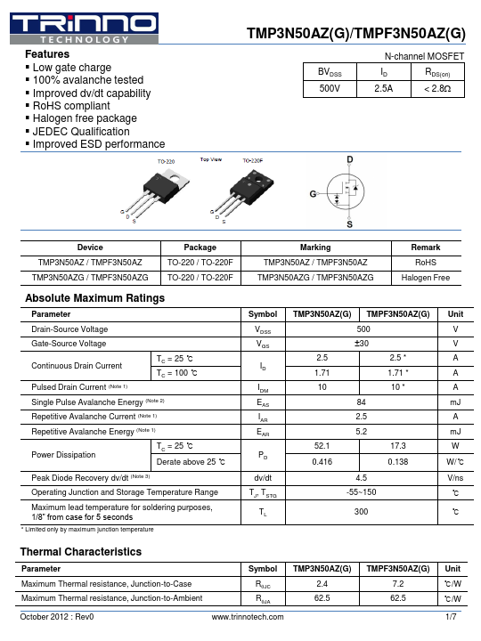
Device TMP3N50AZ / TMPF3N50AZ TMP3N50AZG / TMPF3N50AZG
Package TO-220 / TO-220F TO-220 / TO-220F
Absolute Maximum Ratings
Parameter
Drain-Source Voltage
Gate-Source Voltage Continuous Drain Current Pulsed Drain Current (Note 1)
TC = 25 ℃ TC = 100 ℃
Single Pulse Avalanche Energy (Note 2)
Repetitive Avalanche Current (Note 1)
Repetitive Avalanche Energy (Note 1)
Power Dissipation
TC = 25 ℃ Derate above 25 ℃
Peak Diode Recovery dv/dt (Note 3)
Operating Junction and Storage Temperature Range
Maximum lead temperature for soldering purposes, 1/8” from case for 5 seconds
- Limited only by maximum junction temperature
Marking TMP3N50AZ / TMPF3N50AZ TMP3N50AZG / TMPF3N50AZG
Remark Ro HS
Halogen Free
Symbol VDSS VGS
IDM EAS IAR...