TT 2N3810DCSM
SILICON DUAL MATCHED PNP TRANSISTORS
| Part No. | 2N3810DCSM |
|---|---|
| Datasheet | 2N3810DCSM Download |
| Manufacturer |  TT |
| Description | SILICON DUAL MATCHED PNP TRANSISTORS |
| Buy | Stock & Price |
APPLICATIONS
.● Screening Options Available
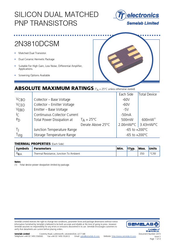
ABSOLUTE MAXIMUM RATINGS
(TA = 25°C unless otherwise stated) Each Side Total Device VCBO Collector – Base Voltage -60V VCEO Collector – Emitter Voltage -60V VEBO Emitter – Base Voltage -5V IC Continuous Collector Current -50mA PD Total Power Dissipation at TA = 25°C 500mW 600mW(1) Derate Above 25°C 2.86mW/°C 3.43mW/°C TJ Junction Temperature Range -65 to +200°C Tstg Storage Temperature Range -65 to +200°C THERMAL PROPERTIES (Each Side) Symbols Parameters RθJA Thermal Resistance, Junction To Ambient Min. 1Typ. Max. Units 350 °C/W Notes (1) Total device power dissipation limited by package. Semelab Limited reserves the right to change test conditions, parameter limits and package dimensions without notice. Information furnished by Semelab is believed to be both accurate and reliable at the time of going to press. However Semelab assumes no responsibility for any errors or omissions discovered in its use. Semelab encourages customers to verify that datasheets are current before placing orders.