TT 2N6851
P-CHANNEL POWER MOSFET
| Part No. | 2N6851 |
|---|---|
| Datasheet | 2N6851 Download |
| Manufacturer |  TT |
| Description | P-CHANNEL POWER MOSFET |
| Buy | Stock & Price |
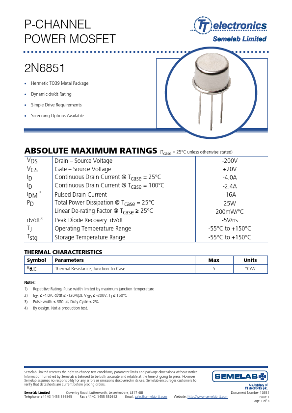
ABSOLUTE MAXIMUM RATINGS
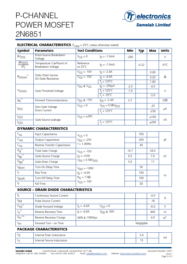
(Tcase = 25°C unless otherwise stated) VDS Drain – Source Voltage -200V VGS Gate – Source Voltage ±20V ID Continuous Drain Current @ Tcase = 25°C -4.0A ID IDM(1) Continuous Drain Current @ Tcase = 100°C Pulsed Drain Current -2.4A -16A PD Total Power Dissipation @ Tcase = 25°C 25W Linear De-rating Factor @ Tcase ≥ 25°C 200mW/°C dv/dt(2) Peak Diode Recovery dv/dt -5V/ns TJ Operating Temperature Range -55°C to +150°C Tstg Storage Temperature Range -55°C to +150°C THERMAL CHARACTERISTICS Symbol Parameters RθJC Thermal Resistance, Junction To Case Max 5 Units °C/W Notes: 1) Repetitive Rating; Pulse width limited by maximum junction temperature 2) ISD ≤ -4.0A, di/dt ≤ -120A/µs, VDD ≤ -200V, TJ ≤ 150°C 3) Pulse width ≤ 380 µs; Duty Cycle ≤ 2% 4) By design. Not a production test. Semelab Limited reserves the right to change test conditions, parameter limits and package dimensions without notice. Information furnished by Semelab is believed to be both accurate and reliable at the time of going to press.