Taiwan Memory Technology T35L3232B
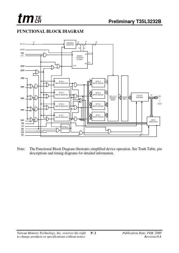
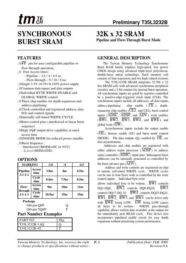
The T35L3232B SRAM integrates 32,768 x 32 bits SRAM cells with advanced synchronous peripheral circuitry and a 2-bit counter for internal burst operation. The synchronous inputs include all addresses, all data inputs, address-pipelining chip enable ( CE ), depthexpansion chip enables (CE2 and CE2), burst control inputs (ADSC , ADSP, and ADV ), write enables ( BW1, BW2 , BW3 , BW4 , and BWE ), and global write (GW ). The data outputs (Q), enabled by OE , are also asynchronous.| Part No. | T35L3232B |
|---|---|
| Datasheet | T35L3232B Download |
| Manufacturer |  Taiwan Memory Technology |
| Description | 32K x 32 SRAM |
| Buy | Stock & Price |
FEATURES
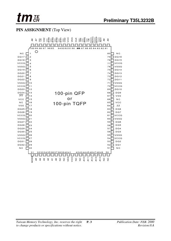
¡E FT pin for user configurable pipeline or flow-through operation. ¡E Fast Access times: - Pipeline – 3.8 / 4 / 4.5 ns - Flow-through – 9 / 10 / 11ns ¡ESingle 3.3V +0.3V/-0.165V power supply ¡ECommon data inputs and data outputs ¡EIndividual BYTE WRITE ENABLE and GLOBAL WRITE control ¡E Three chip enables for depth expansion and address pipelining ¡E Clock-controlled and registered address, data I/Os and control signals ¡EInternally self-timed WRITE CYCLE ¡EBurst control pins ( interleaved or linear burst sequence) ¡EHigh 30pF output drive capability at rated access time ¡ESNOOZE MODE for reduced power standby ¡E Burst Sequence : - Interleaved (MODE=NC or VCC) - Linear (MODE=GND) OPTIONS MARKING -3.8 -4 Pipeline 3-1-1-1 Access time Cycle time Flowthrough 2-1-1-1 Access time Cycle time 3.8ns 6.6ns 9ns 10.5ns 4ns 7.5ns 10ns 15ns Package 100-pin QFP Q 100-pin TQFP T Part Number Examples PART NO. Pkg. T35L3232B-3.8Q Q T35L3232B-4T T -4.5 4.5ns 8.5ns 11ns 15nsGENERAL DESCRIPTION
...