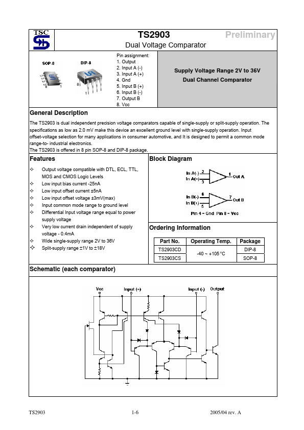
GENERAL DESCRIPTION
Input offset-voltage selection for many applications in consumer automotive, and It is designed to permit a common mode range-to- industrial electronics. FEATURES
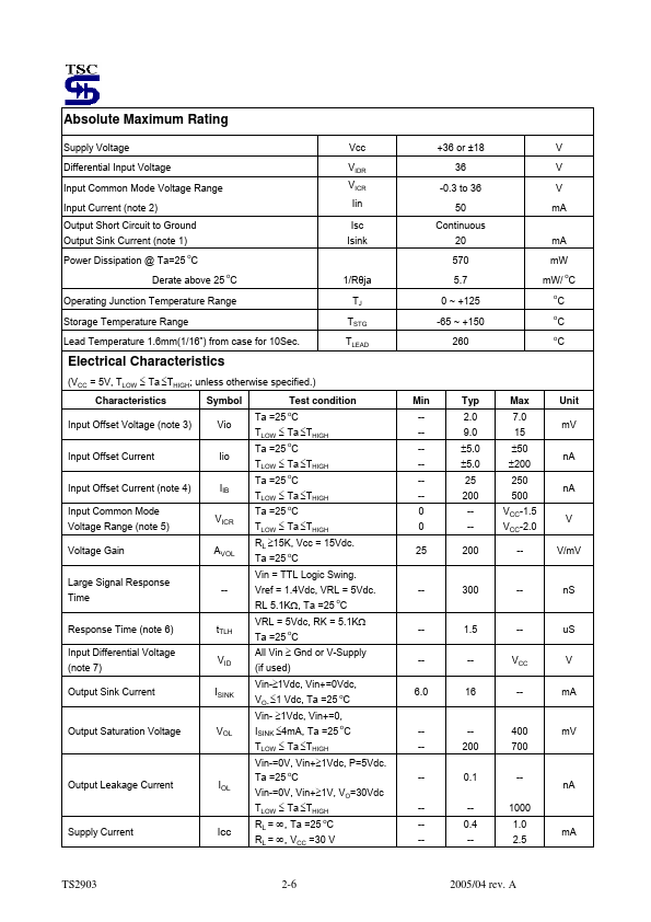
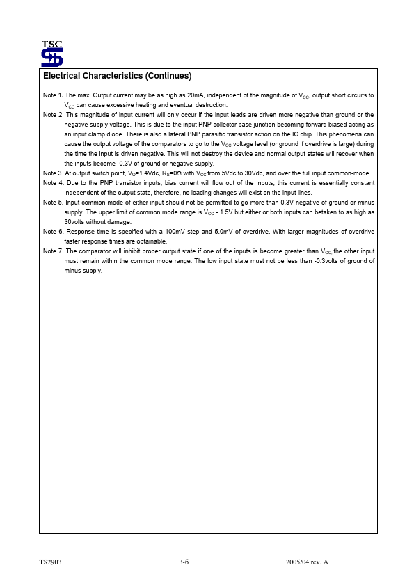
Output voltage compatible with DTL, ECL, TTL, MOS and CMOS Logic Levels Low input bias current -25nA Low input offset current ±5nA Low input offset voltage ±3mV(max) Input common mode range to ground level Differential lnput voltage range equal to power supply voltage Very low current drain independent of supply voltage - 0.4mA Wide single-supply range 2V to 36V Split-supply range ±1V to ±18V Block Diagram Ordering Information Part No. TS2903CD TS2903CS Operating Temp. o -40 ~ +105 C Package DIP-8 SOP-8 Schematic (each comparator) TS2903 1-6 2005/04 rev. A Absolute Maximum Rating Supply Voltage Differential Input Voltage Input Common Mode Voltage Range Input Current (note 2) Output Short Circuit to Ground Output Sink Current (note 1) Power Dissipation @ Ta=25 oC Derate above 25 C Operatin... Taiwan Semiconductor