Taiwan Semiconductor TSM500N03
N-Channel Power MOSFET
| Part No. | TSM500N03 |
|---|---|
| Datasheet | TSM500N03 Download |
| Manufacturer |  Taiwan Semiconductor |
| Description | N-Channel Power MOSFET |
| Buy | Stock & Price |
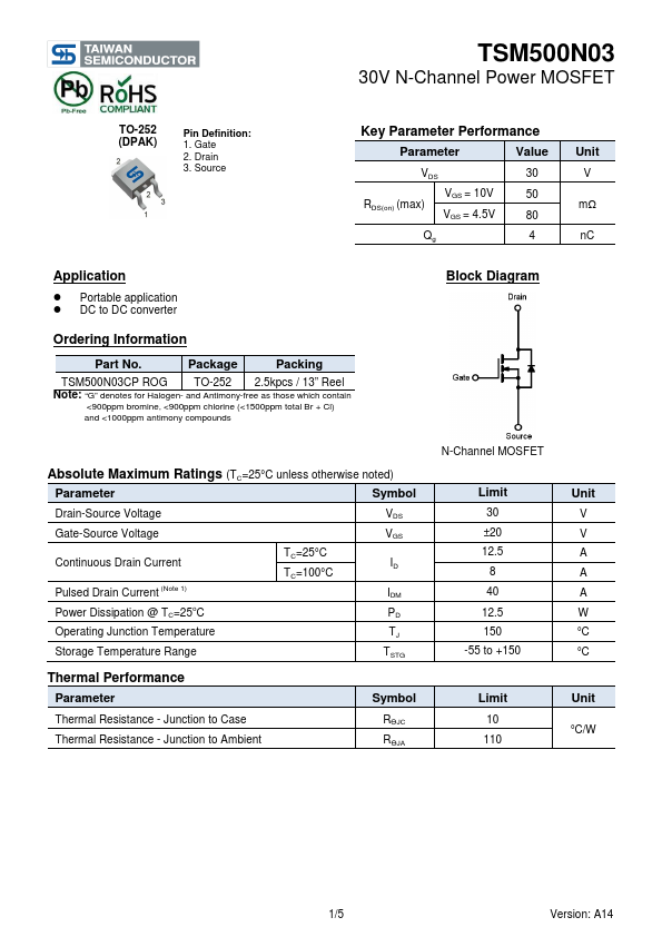
ABSOLUTE MAXIMUM RATINGS
(TC=25°C unless otherwise noted) Parameter Symbol Drain-Source Voltage VDS Gate-Source Voltage VGS Continuous Drain Current Pulsed Drain Current (Note 1) Power Dissipation @ TC=25oC TC=25°C TC=100°C ID IDM PD Operating Junction Temperature TJ Storage Temperature Range TSTGTHERMAL PERFORMANCE
Parameter Symbol Thermal Resistance - Junction to Case Thermal Resistance - Junction to Ambient RӨJC RӨJA N-Channel MOSFET Limit 30 ±20 12.5 8 40 12.5 150 -55 to +150 Limit 10 110 Unit V V A A A W °C °C Unit °C/W 1/5 Version: A14 TSM500N03 30V N-Channel Power MOSFETELECTRICAL SPECIFICATIONS
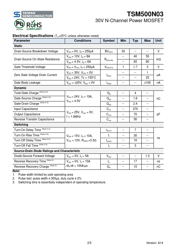
(TC=25°C unless otherwise noted) Parameter Conditions Symbol Static Drain-Source Breakdown Voltage Drain-Source On-State Resistance Gate Threshold Voltage VGS = 0V, ID = 250µA VGS = 10V, ID = 8A VGS = 4.5V, ID = 8A VDS = VGS, ID = 250µA BVDSS RDS(ON) VGS(TH) Zero Gate Voltage Drain Current Gate Body Leakage Dynamic Total Gate Charge (Note 2,3) Gate-Source Charge (Note 2,3) Gate-Drain C...