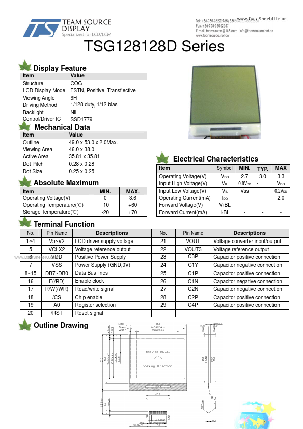
Item Operating Voltage(V) Input High Voltage(V) Input Low Voltage(V) Operating Current(mA) Forward Voltage(V) Forward Current(mA) Symbol VDD VIH VIL IDD Vf BL If BL MIN. 2.7 0.8VDD Vss - Absolute Maximum Item Operating Voltage(V) Operating Temperature(℃) Storage Temperature(℃) MIN. 0 -10 -20 MAX. 3.6 +60 +70 TYP. 3.0 - MAX 3.3 VDD 0.2VDD 2.0 - Terminal Function No. 1~4 5 7 8~15 16 17 18 19 20 Pin Name V5~V2 VCLX2 VSS DB7~DB0 E(/RD) R/W(/WR) /CS A0 /RST Descriptions LCD driver supply voltage Voltage reference output Positive Power Supply Power Supply (GND,0V) Data Bus lines Enable clock Read/write signal Chip enable Register selection Reset signal No. 21 22 23 24 25 26 27 28 29 Pin Name VOUT VOUT3 C3P C1Y C1P C1N C2N C2P C4P Descriptions Voltage converter input/output Voltage reference output Capacitor positive connection Capacitor negative connection Capacitor positive connection Capacitor negative connection Capacitor negative connection Capa...
This website uses cookies or similar technologies, to enhance your browsing experience and provide personalized recommendations. By continuing to use our website, you agree to our Privacy Policy