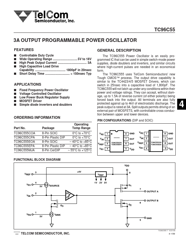
FEATURES
s s s s s Controllable Duty Cycle Wide Operating Range ............................. 5V to 18V High Peak Output Current .................................. 3A High Capacitive Load Drive Capability .................................... 1800pF in 20nsec Short Delay Time ............................. < 150nsec Typ GENERAL DESCRIPTION
The TC96C555 will not latch up under any conditions within their power and voltage ratings. They can accept, without damage, up to 1.5A of reverse current (of either polarity) being forced back into the output. All terminals are also fully protected against up to 4kV of electrostatic discharge. The peak output is rated at 3A. Split outputs permits driving of an external pair of MOSFETS, with controllable cross conduction between upper and lower devices. PIN CONFIGURATIONS (DIP and SOIC) Operating Temp Range 0°C to +70°C 0°C to +70°C – 40°C to +85°C – 40°C to +85°C – 55°C to +125°C VR2 VIN VREF VR1 1 2 3 4 TC96C555CPA TC96C555EPA 2 3 4 5 6 APPLICATIONS
... TelCom Semiconductor