SMD10P06L Overview
Key Specifications
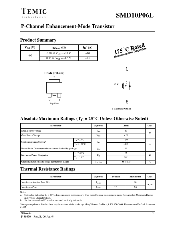
Max Operating Temp: 175 °C
Key Features
- 10 V 0.35 @ VGS =
- 48 V, VGS = 0 V
| Part | SMD10P06L |
|---|---|
| Description | P-Channel Transistor |
| Category | Transistor |
| Manufacturer | TEMIC Semiconductors |
| Size | 62.50 KB |
Max Operating Temp: 175 °C
| Seller | Inventory | Price Breaks | Buy |
|---|---|---|---|
| Component Stockers USA | 411 | 1+ : 99.99 USD | View Offer |
| Best Source | 6414 | 1+ : 0.2353 USD | View Offer |
| Part Number | Manufacturer | Description |
|---|---|---|
| BDT88 | Inchange Semiconductor | Silicon PNP Power Transistor |
| KD333 | Tesla Elektronicke | Transistor |
| C828 | SEMTECH | NPN Silicon Transistor |