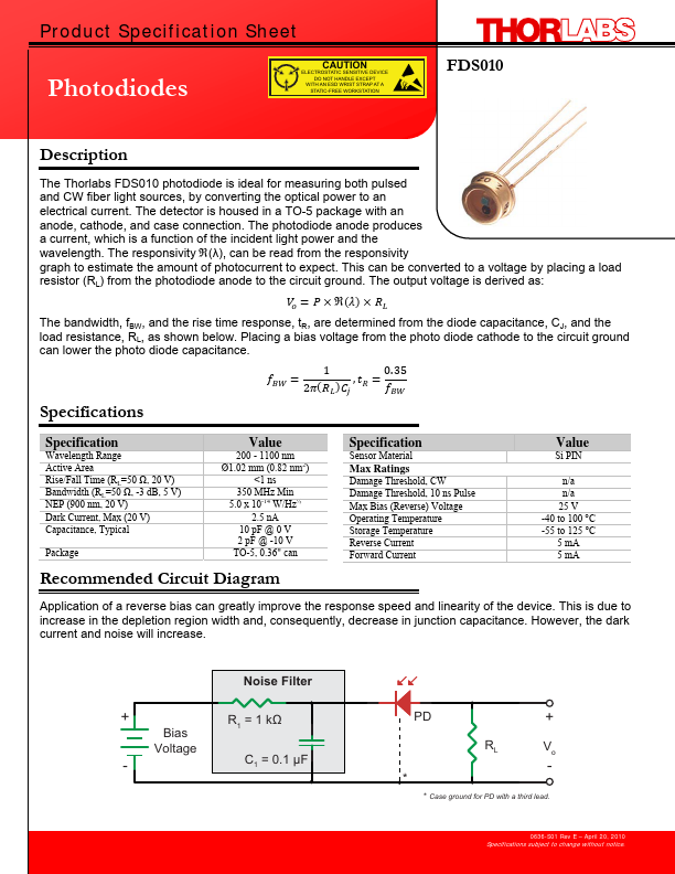
DESCRIPTION
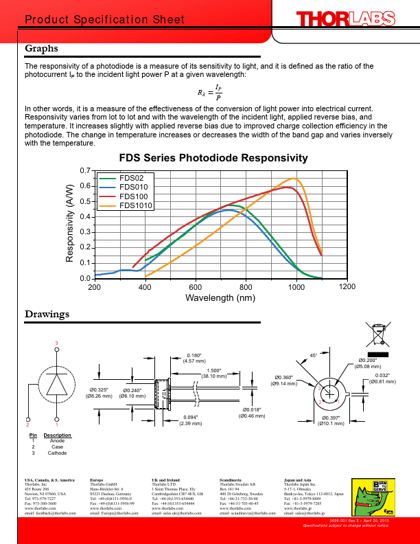
The photodiode anode produces a current, which is a function of the incident light power and the wavelength. The responsivity (λ), can be read from the responsivity graph to estimate the amount of photocurrent to expect. This can be converted to a voltage by placing a load resistor (RL) from the photodiode anode to the circuit ground. The output voltage is derived as: The bandwidth, fBW, and the rise time response, tR, are determined from the diode capacitance, CJ, and the load resistance, RL, as shown below. Placing a bias voltage from the photo diode cathode to the circuit ground can lower the photo diode capacitance. 1 0.35 , 2 Specifications Specification Wavelength Range Active Area Rise/Fall Time (RL=50 Ω, 20 V) Bandwidth (RL=50 Ω, -3 dB, 5 V) NEP (900 nm, 20 V) Dark Current, Max (20 V) Capacitance, Typical Package Value 200 - 1100 nm Ø1.02 mm (0.82 nm2) <1 ns 350 MHz Min 5.0 x 10⁻¹⁴ W/Hz½ 2.5 nA 10 pF @ 0 V 2 pF @ -10 V TO-5, 0.36" can Recommended Circuit Diagram Spe...