TOREX SEMICONDUCTOR XC66D
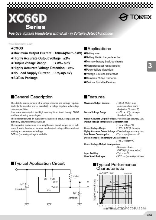
The XC66D series consists of a voltage detector and voltage regulator built into the one chip and is, essentially, a voltage regulator with voltage detect capabilities. The detector features an output driver, hysteresis circuit, comparator and extremely accurate standard voltage. The regulator features an error amplification circuit, output driver with current limiter functions, minimal input-output voltage differential and similary accurate standard voltage.| Part No. | XC66D |
|---|---|
| Datasheet | XC66D Download |
| Manufacturer |  TOREX SEMICONDUCTOR |
| Description | Positive Voltage Regulators |
| Buy | Stock & Price |
DESCRIPTION
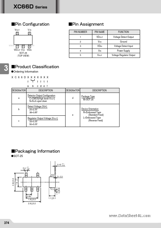
Detector Output Configuration C=CMOS(High level=VOUT) N=N-ch open drain Detect Voltage (VDF) 25=2.5V 38=3.8V DESIGNATOR dDESCRIPTION
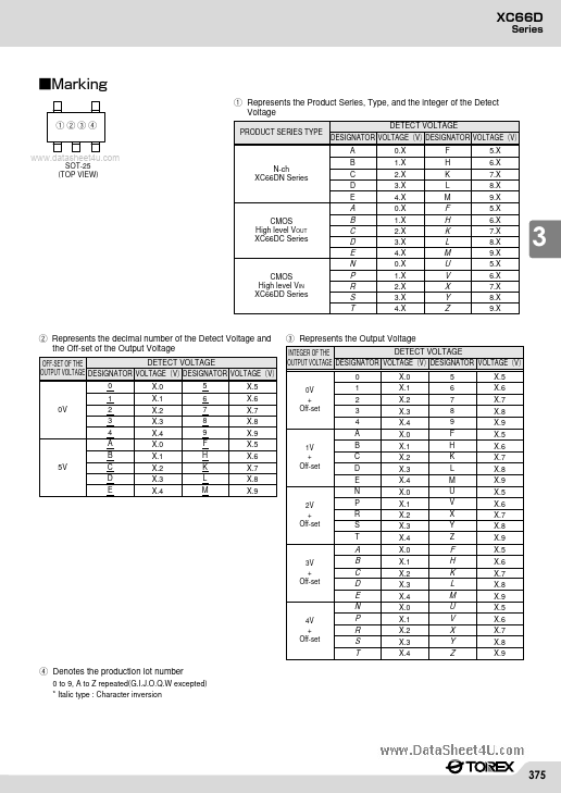
Package Type M=SOT-25 b e c Regulator Output Voltage (VOUT) 33=3.3V 50=5.0V Device Orientation R=Embossed Tape (Standard Feed) L=Embossed Tape (Reverse Feed) GSOT-25 374 q qwer 3 w e r 375 (1) XC66DC CMOS output (High level =VOUT) (2) XC66DN N-ch open drain 3 Ta=25 °C PARAMETER Regulator Input Voltage Regulator Output Current Regulator Output Voltage Detector Input Voltage Detector Output Current Detector Output Voltage N-ch open drain output SYMBOL VIN IOUT VOUT VDIN IDOUT VDOUT RATINGS VSS -0.3 ~ 12 150 VSS -0.3 ~ VIN +0.3 VSS -0.3 ~ 12 50 VSS -0.3 ~ 12 UNITS V mA V V mA V CMOS output (High level =VOUT) Pd Topr Tstg VSS -0.3 ~ VIN +0.3 150 -30 ~ +80 -40 ~ +125 mW °C °C Continuous Total Power Dissipation Operating Ambient Temperature Storage Temperature Note: Please ensure that {(VIN -VOUT ) x IOUT} + {IDOUT x VDOUT} + {VIN x ISS} does not exceed the stated Pd values.