XC8113
Description
The XC8112/XC8113 series are 2ch load switch IC with ideal diode function.
Key Features
- Input Voltage Range Output Current
Applications
- Wearable devices
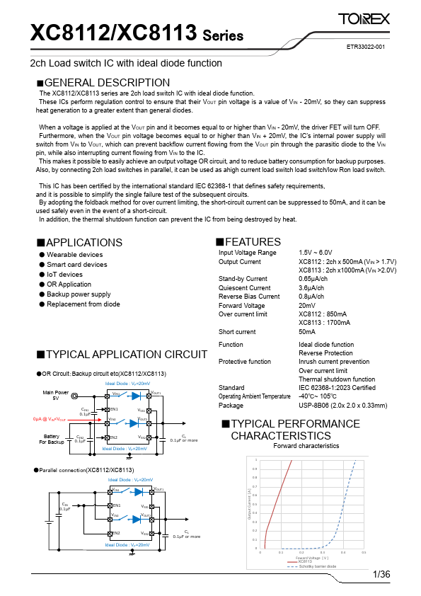
The XC8112/XC8113 series are 2ch load switch IC with ideal diode function.