2SJ537
TOSHIBA Field Effect Transistor Silicon P Channel MOS Type (L2- π- MOSVI)
Chopper Regulator, DC- DC Converter and Motor Drive Applications
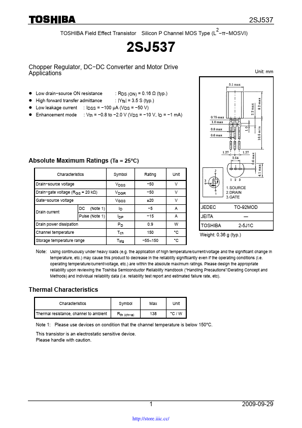
Unit: mm z Low drain- source ON resistance
: RDS (ON) = 0.16 Ω (typ.) z High forward transfer admittance
: |Yfs| = 3.5 S (typ.) z Low leakage current : IDSS =
- 100 μA (VDS =
- 50 V) z Enhancement mode : Vth =
- 0.8 to
- 2.0 V (VDS =
- 10 V, ID =
- 1 m A)
Absolute Maximum Ratings (Ta = 25°C)
Characteristics
Symbol
Rating
Unit
Drain- source voltage
Drain- gate voltage (RGS = 20 kΩ) Gate- source voltage
Drain current
DC (Note 1) Pulse (Note 1)
Drain power dissipation
Channel temperature
Storage temperature range
VDSS VDGR VGSS
ID IDP PD Tch Tstg
- 50
- 50 ±20
- 5
- 15 0.9 150
- 55~150
V V V A A W °C °C
JEDEC
TO-92MOD
JEITA
―
TOSHIBA
2-5J1C
Weight: 0.36 g (typ.)
Note: Using continuously under heavy loads (e.g. the application of high temperature/current/voltage and the significant change in temperature, etc.) may cause this...