2SK3633
2SK3633 is N-Channel MOSFET manufactured by Toshiba.
TOSHIBA Field Effect Transistor Silicon N-Channel MOS Type (π- MOS IV)
..
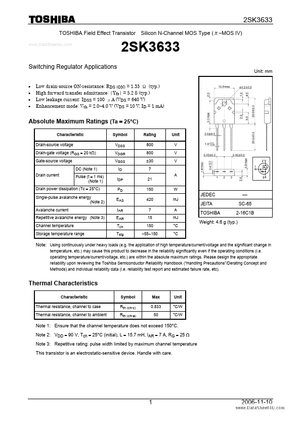
Unit: mm
Switching Regulator Applications
- -
- - Low drain-source ON-resistance: RDS (ON) = 1.35 Ω (typ.) High forward transfer admittance: |Yfs| = 5.2 S (typ.) Low leakage current: IDSS = 100 μA (VDS = 640 V) Enhancement mode: Vth = 2.0~4.0 V (VDS = 10 V, ID = 1 m A)
Absolute Maximum Ratings (Ta = 25°C)
Characteristic Drain-source voltage Drain-gate voltage (RGS = 20 kΩ) Gate-source voltage DC (Note 1) Drain current Pulse (t = 1 ms) (Note 1) Symbol VDSS VDGR VGSS ID IDP PD EAS IAR EAR Tch Tstg Rating 800 800 ±30 7 21 150 420 7 15 150
- 55~150 A W Unit V V V
Drain power dissipation (Tc = 25°C) Single-pulse avalanche energy (Note 2) Avalanche current Repetitive avalanche energy (Note 3) Channel temperature Storage temperature range
JEDEC m J A m J °C °C
⎯ SC-65 2-16C1B
JEITA TOSHIBA
Weight: 4.6 g (typ.)
Note: Using continuously under heavy loads (e.g. the application of high temperature/current/voltage and the significant change in temperature, etc.) may cause this product to decrease in the reliability significantly even if the operating conditions (i.e. operating temperature/current/voltage, etc.) are within the absolute maximum ratings. Please design the appropriate reliability upon reviewing the Toshiba Semiconductor Reliability Handbook (“Handling Precautions”/Derating Concept and Methods) and individual reliability data (i.e. reliability test report and estimated failure rate, etc).
Thermal Characteristics
Characteristic Thermal resistance, channel to case Thermal resistance, channel to ambient Symbol Rth (ch-c) Rth (ch-a) Max 0.833 50 Unit °C/W °C/W
Note 1: Ensure that the channel temperature does not exceed 150°C. Note 2: VDD = 90 V, Tch = 25°C (initial), L = 15.7 m H, IAR = 7 A, RG = 25 Ω Note 3: Repetitive rating: pulse width limited by maximum channel temperature This transistor is an electrostatic-sensitive device. Handle with care.
2006-11-10
Elec...