Datasheet4U.com
🌙
JBT6K49-AS Datasheet | Toshiba
Part:
JBT6K49-AS
Description:
Power supply IC
Manufacturer:
Toshiba
Size:
226.15 KB
JBT6K49-AS Datasheet (PDF) Download
Toshiba
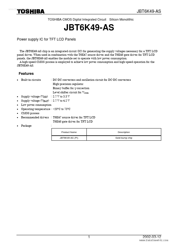
JBT6K49-AS
Key Features
VREF VREFIN VSOUT2
×
Close