K11A65D
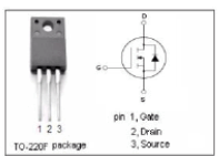
Representative K11A65D image (package may vary by manufacturer)
Overview
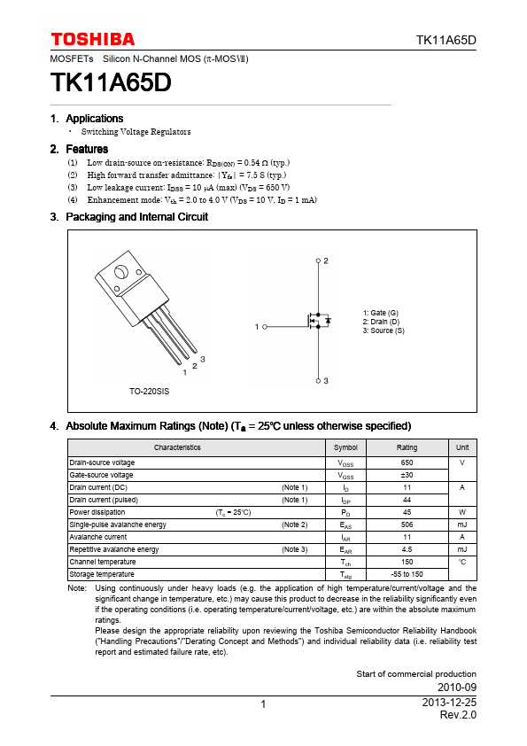
- Packaging and Internal Circuit TK11A65D 1: Gate (G) 2: Drain (D) 3: Source (S)
| Part | K11A65D |
|---|---|
| Description | TK11A65D |
| Manufacturer | Toshiba |
| Size | 324.75 KB |
Representative K11A65D image (package may vary by manufacturer)
| Part Number | Manufacturer | Description |
|---|---|---|
| HFDOM40B-xxxSx | Hanbit Electronics | 40Pin Flash Disk Module |
| HFDOM44P-xxxSx | Hanbit Electronics | 44Pin Flash Disk Module |
| BDT88 | Inchange Semiconductor | Silicon PNP Power Transistor |