K30A06J3A
Overview
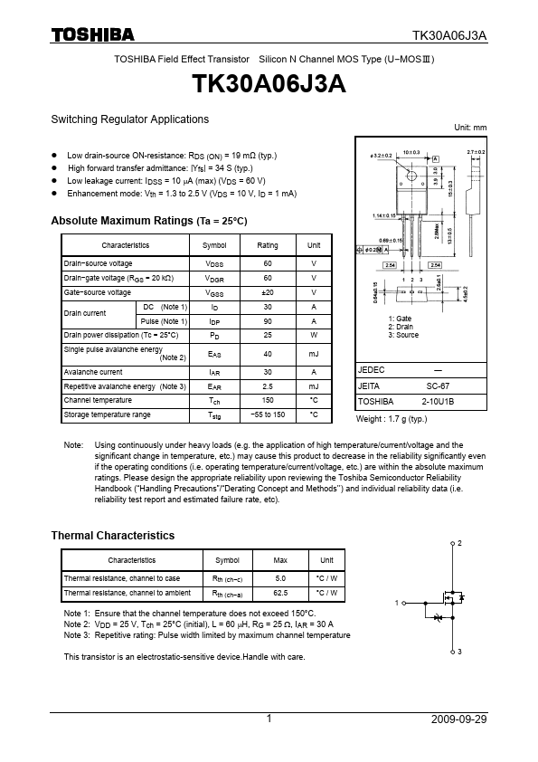
TK30A06J3A TOSHIBA Field Effect Transistor Silicon N Channel MOS Type (U−MOSⅢ) TK30A06J3A Switching Regulator Applications Unit: mm z Low drain-source ON-resistance: RDS (ON) = 19 mΩ (typ.) z High ...
| Part | K30A06J3A |
|---|---|
| Description | TK30A06J3A |
| Manufacturer | Toshiba |
| Size | 190.16 KB |
TK30A06J3A TOSHIBA Field Effect Transistor Silicon N Channel MOS Type (U−MOSⅢ) TK30A06J3A Switching Regulator Applications Unit: mm z Low drain-source ON-resistance: RDS (ON) = 19 mΩ (typ.) z High ...
| Part Number | Manufacturer | Description |
|---|---|---|
| HFDOM40B-xxxSx | Hanbit Electronics | 40Pin Flash Disk Module |
| HFDOM44P-xxxSx | Hanbit Electronics | 44Pin Flash Disk Module |
| BDT88 | Inchange Semiconductor | Silicon PNP Power Transistor |