SSM3J317T Overview
Key Features
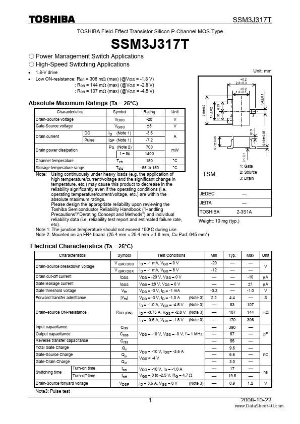
- 1.8-V drive Low ON-resistance: Ron = 306 mΩ (max) (@VGS = -1.8 V) : Ron = 144 mΩ (max) (@VGS = -2.8 V) : Ron = 107 mΩ (max) (@VGS = -4.5 V)
| Part | SSM3J317T |
|---|---|
| Description | Power Management Switch Applications High-Speed Switching Applications |
| Category | Power Management IC |
| Manufacturer | Toshiba |
| Size | 237.29 KB |
| Part Number | Manufacturer | Description |
|---|---|---|
| i.MX28 | NXP Semiconductors | Applications Processors |
| I.MX31 | Freescale Semiconductor | Multimedia Applications Processors |
| i.MX35 | Freescale Semiconductor | Applications Processors |