TA4019F
Features
- -
- High gain: |S21|2 = 30d B (@45 MHz) Low distortion: IM3 = 53d B (@45 MHz) Operating supply voltage: VCC = 4.75 V~5.25 V
Maximum Ratings (Ta = 25°C)
Characteristics Supply voltage Total power dissipation Operating temperature Storage temperature Symbol VCC PD (Note 1) Topr Tstg 2 Rating 5.5 550 -40~85 -55~150 Unit V m W °C °C
Weight:
0.02g (typ.)
Note 1: When mounted on the glass epoxy 2.5cm ´ 0.4 t
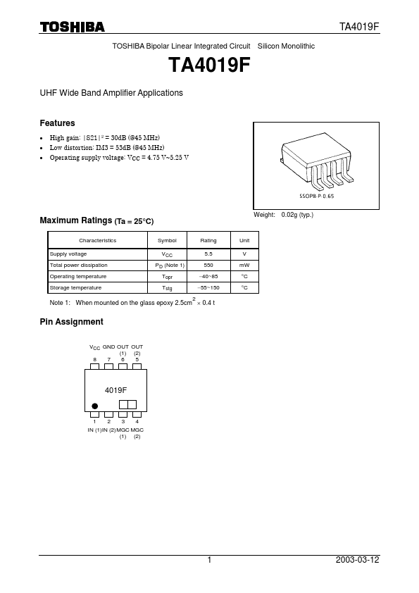
Pin Assignment
VCC GND OUT OUT (1) (2) 8 7 6 5
4019F
IN (1)IN (2)MGC MGC (1) (2)
2003-03-12
Electrical Characteristics (Ta = 25°C, VCC = 5 V, Zg = Zl = 50 W)
Characteristics Circuit current Band width Input return loss Insertion gain (1) Insertion gain (2) Isolation Output return loss Noise figure 3 rd
Symbol Icc BW |S11|
2 2
Test Circuit
Test Condition Non carrier
Min 28
Typ. 35 300 -0.3 30 10.5 -57 -2.1 8 53
Max 42 ¾ ¾ 33 13.5 ¾ ¾ 11 ¾
Unit m A MHz d B d B d B d B d B d B d B
Fig2
(Note 2) f = 45MHz f = 45MHz
200 ¾ 27 7.5 ¾ ¾ ¾ 47
|S21| (1)...