TA8483CP
TA8483CP is Three-Phase All wave Driver manufactured by Toshiba.
TOSHIBA Bipolar Linear Integrated Circuit Silicon Monolithic
Three- Phase All wave Driver IC
The TA8483CP is a three- phase all wave driver IC that makes possible PWM sensorless driving.
Features
- Built- in excess current detection function
- Built- in heat protection function
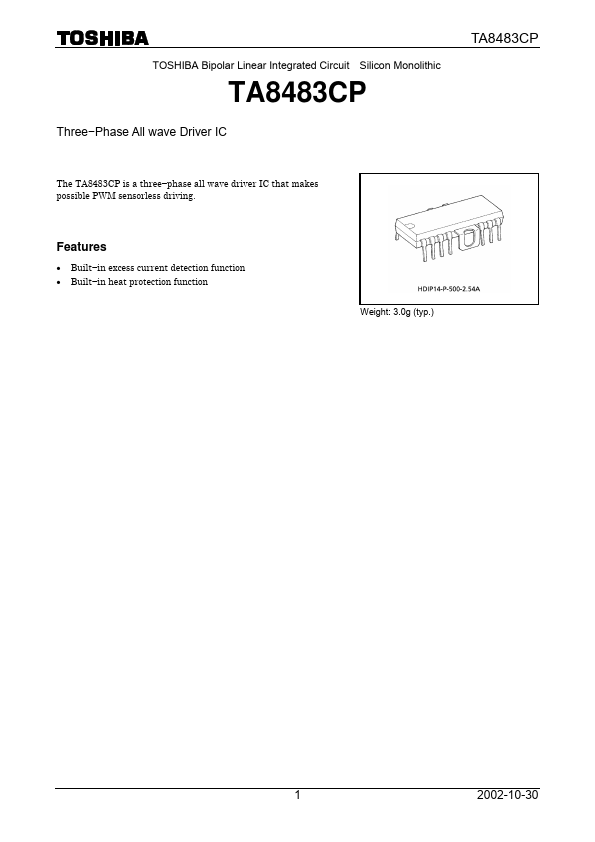
Weight: 3.0g (typ.)
1 2002-10-30
Block Diagram
- SEL 2
Heat protection
N P 34
Output voltage detection circuit
VCC 10
IN- U 11 IN- V 12 IN- W 13
Control circuit
Excess current detection
1 ISD
5,FIN
9 OUT- U 7 OUT- V 6 OUT- W
VI 8 14 VISD
2 2002-10-30
Pin Connection
ISD TSD- SEL
1 2 3 4
GND OUT- W OUT- V
5 6 7
14 VISD 13 IN- W 12 IN- V 11 IN- U
10...