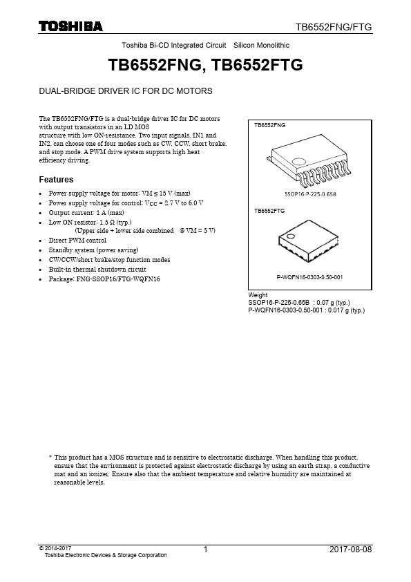
Datasheet4U Logo Datasheet4U.com

TB6552FNG - Dual-Bridge Driver

General Description

Control signal input 1 (Ch.

Control signal input 2 (Ch.

PWM control signal input pin (Ch.

Key Features

  • Power supply voltage for motor: VM ≤ 15 V (max).
  • Power supply voltage for control: VCC = 2.7 V to 6.0 V.
  • Output current: 1 A (max).
  • Low ON resistor: 1.5 Ω (typ. ) (Upper side + lower side combined @ VM = 5 V).
  • Direct PWM control.
  • Standby system (power saving).
  • CW/CCW/short brake/stop function modes.
  • Built-in thermal shutdown circuit.
  • Package: FNG-SSOP16/FTG-WQFN16 TB6552FNG TB6552FTG P-WQFN16-0303-0.50-001 Weight S.

📥 Download Datasheet

Full PDF Text Transcription (Reference)

The following content is an automatically extracted verbatim text from the original manufacturer datasheet and is provided for reference purposes only.

View original datasheet text
TB6552FNG/FTG Toshiba Bi-CD Integrated Circuit Silicon Monolithic TB6552FNG, TB6552FTG DUAL-BRIDGE DRIVER IC FOR DC MOTORS The TB6552FNG/FTG is a dual-bridge driver IC for DC motors with output transistors in an LD MOS structure with low ON-resistance. Two input signals, IN1 and IN2, can choose one of four modes such as CW, CCW, short brake, and stop mode. A PWM drive system supports high heat efficiency driving. Features • Power supply voltage for motor: VM ≤ 15 V (max) • Power supply voltage for control: VCC = 2.7 V to 6.0 V • Output current: 1 A (max) • Low ON resistor: 1.5 Ω (typ.