TC551001BFTL-70L
TC551001BFTL-70L is SILICON GATE CMOS STATIC RAM manufactured by Toshiba.
- Part of the TC551001 comparator family.
- Part of the TC551001 comparator family.
Description
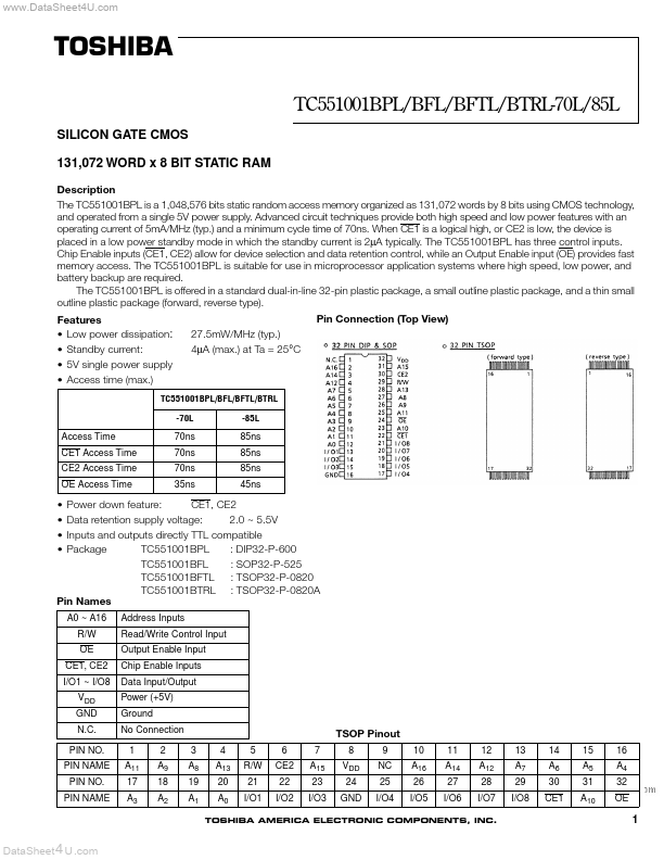
The TC551001BPL is a 1,048,576 bits static random access memory organized as 131,072 words by 8 bits using CMOS technology, and operated from a single 5V power supply. Advanced circuit techniques provide both high speed and low power features with an operating current of 5m A/MHz (typ.) and a minimum cycle time of 70ns. When CE1 is a logical high, or CE2 is low, the device is placed in a low power standby mode in which the standby current is 2µA typically. The TC551001BPL has three control inputs. Chip Enable inputs (CE1, CE2) allow for device selection and data retention control, while an Output Enable input (OE) provides fast memory access. The TC551001BPL is suitable for use in microprocessor application systems where high speed, low power, and battery backup are required.
The TC551001BPL is offered in a standard dual-in-line 32-pin plastic package, a small outline plastic package, and a thin small outline plastic package (forward, reverse type).
Features
Pin Connection (Top View)
- Low power dissipation: 27.5m W/MHz (typ.)
- Standby current:
4µA (max.) at Ta = 25°C
- 5V single power supply
- Access time (max.)
TC551001BPL/BFL/BFTL/BTRL
-70L -85L
Access Time CE1 Access Time CE2 Access Time OE Access Time
70ns 70ns 70ns 35ns
85ns 85ns 85ns 45ns
- Power down feature
:
CE1, CE2
- Data retention supply voltage: 2.0 ~ 5.5V
- Inputs and outputs directly TTL patible
- Package
TC551001BPL : DIP32-P-600
Pin Names
TC551001BFL TC551001BFTL TC551001BTRL
: SOP32-P-525 : TSOP32-P-0820 : TSOP32-P-0820A
A0 ~ A16 Address Inputs
R/W Read/Write Control Input
OE Output Enable Input
CE1, CE2 Chip Enable Inputs
I/O1 ~ I/O8 Data Input/Output
VDD GND
Power (+5V) Ground
N.C. No Connection
TSOP Pinout
PIN NO. 1 2 3 4 5 6 7 8 9 10 11 12 13 14 15 16
PIN NAME A11 A9 A8 A13 R/W CE2 A15 VDD NC A16 A14 A12 A7 A6 A5 A4 PIN NO. 17 18 19 20 21 22 23 24 25 26 27 28 29 30 31 32
PIN NAME A3 A2 A1 A0 I/O1 I/O2 I/O3 GND I/O4 I/O5 I/O6 I/O7 I/O8 CE1 A10...