TC55V16256FTI-15
TC55V16256FTI-15 is MOS DIGITAL INTEGRATED CIRCUIT SILICON GATE CMOS manufactured by Toshiba.
- Part of the TC55V16256FTI-12 comparator family.
- Part of the TC55V16256FTI-12 comparator family.
TC55V16256JI/FTI-12,-15
TOSHIBA MOS DIGITAL INTEGRATED CIRCUIT SILICON GATE CMOS
262,144-WORD BY 16-BIT CMOS STATIC RAM DESCRIPTION
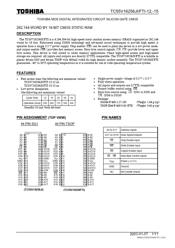
The TC55V16256JI/FTI is a 4,194,304-bit high-speed static random access memory (SRAM) organized as 262,144 words by 16 bits. Fabricated using CMOS technology and advanced circuit techniques to provide high speed, it operates from a single 3.3 V power supply. Chip enable ( CE ) can be used to place the device in a low-power mode, and output enable ( OE ) provides fast memory access. Data byte control signals ( LB , UB ) provide lower and upper byte access. This device is well suited to cache memory applications where high-speed access and high-speed storage are required. All inputs and outputs are directly LVTTL patible. The TC55V16256JI/FTI is available in plastic 44-pin SOJ and 44-pin TSOP with 400mil width for high density surface assembly. The TC55V16256JI/FTI guarantees
- 40° to 85°C operating temperature so it is suitable for use in wide operating temperature system.
..
Features
- Fast access time (the following are maximum values) TC55V16256JI/FTI-12:12 ns TC55V16256JI/FTI-15:15 ns Low-power dissipation (the following are maximum values)
Cycle Time Operation (max) 12 230 15 200 20 170 25 150 ns m A
- -
- -
- -
- Standby:10 m A (both devices)
Single power supply voltage of 3.3 V ± 0.3 V Fully static operation All inputs and outputs are LVTTL patible Output buffer control using OE Data byte control using LB (I/O1 to I/O8) and UB (I/O9 to I/O16) Package: SOJ44-P-400-1.27 (JI) (Weight: 1.64 g typ) TSOP II44-P-400-0.80 (FTI) (Weight: 0.45 g typ)
PIN ASSIGNMENT (TOP VIEW)
44 PIN SOJ 44 PIN TSOP
PIN NAMES
A0 to A17 A4 A3 A2 A1 A0 CE I/O1 I/O2 I/O3 I/O4 VDD GND I/O5 I/O6 I/O7 I/O8 WE A15 A14 A13 A12 A16 1 2 3 4 5 6 7 8 9 10 11 12 13 14 15 16 17 18 19 20 21 22 44 43 42 41 40 39 38 37 36 35 34 33 32 31 30 29 28 27 26 25 24 23 A5 A6 A7 OE UB LB I/O16 I/O15 I/O14 I/O13 GND VDD I/O12 I/O11 I/O10 I/O9 NU A8 A9...


