TC59LM836DMB
Overview
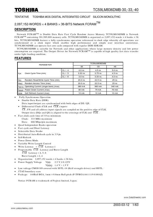
- Fully Synchronous Operation
- Double Data Rate (DDR) Data input/output are synchronized with both edges of DS / QS.
- Differential Clock (CLK and CLK ) inputs CS , FN and all address input signals are sampled on the positive edge of CLK. Output data (DQs and QS) is aligned to the crossings of CLK and CLK . Fast clock cycle time of 3.0 ns minimum Clock: 333 MHz maximum Data: 666 Mbps/pin maximum Quad Independent Banks operation Fast cycle and Short Latency Selectable Data Strobe Distributed Auto-Refresh cycle in 3.9 µs Self-Refresh Power Down Mode Variable Writ