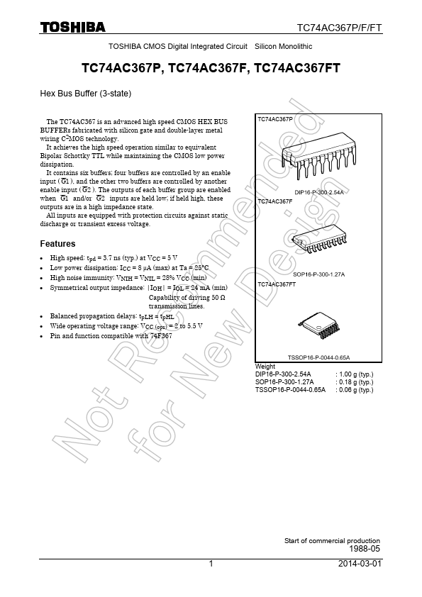
TC74AC367P
TC74AC367P is manufactured by Toshiba.
TC74AC367P/F/FT
TOSHIBA CMOS Digital Integrated Circuit Silicon Monolithic
TC74AC367P, TC74AC367F, TC74AC367FT
Hex Bus Buffer (3-state)
The TC74AC367 is an advanced high speed CMOS HEX BUS BUFFERs fabricated with silicon gate and double-layer metal wiring C2MOS technology.
It achieves the high speed operation similar to equivalent Bipolar Schottky TTL while maintaining the CMOS low power dissipation.
It contains six buffers; four buffers are controlled by an enable input ( G1 ), and the other two buffers are controlled by another enable input ( G2 ). The outputs of each buffer group are enabled when G1 and/or G2 inputs are held low; if held high, these outputs are in a high impedance...